Hey everyone! This blog will cover the following: -
- System Overview
- Use-case
- What are Outbound and Inbound windows in PCIe and how do they work?
- What is ATU and why is it important in PCIe?
- How to configure the PCIe windows in LS1028 and iMX8QXP
- Code walkthrough
- Running the test case
System Overview

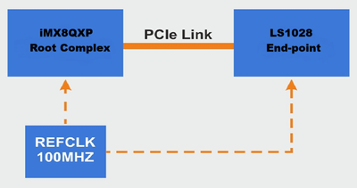
As depicted in the illustration above, the system has 2 main blocks: -
a. iMX8QXP [configured as PCIe Root Complex]
b. LS1028 [ configured as PCIe Endpoint]
Software components: -
iMX8QXP - Linux Factory 6.6.36
LS1028ARDB - LSDK-18.09
Hardware components: -
iMX8QXP MEK Board
LS1028ARDB Board
M.2 Key E PCIe Bridge
The root complex and endpoint are connected via a PCIe bridge on M.2 Key E connector of both the boards.
Reference clock used for both PCIe RC and EP - 100 MHz
 PCIe Bridge with M.2 Key E interface
M.2 Key E PCIe Bridge
Use-case
There was a customer requirement wherein a software program was needed at Uboot to benchmark the PCIe to DDR transfers, involving cacheable and non-cacheable DRAM memory regions.
The benchmark software periodically realizes several DMA transfers from PCIe space to DDR in the following way: -
1) Start PCIe to DDR DMA transfer (no descriptor). Data are transferred from PCIe to a non-cacheable buffer (A).
2) Wait for the DMA transfer to finish.
3) Copy received data from non-cacheable buffer (A) to a cacheable buffer(B).
4) Check if there's a data mismatch and reports accordingly.
Note: -
There are 2 types of DMA transfers - Descriptor and Non-descriptor.
In Descriptor based DMA, the CPU sets up a list or chain of 'descriptors' in memory. Each descriptor is a data structure containing info such as source, destination, transfer size etc.
In Non-descriptor DMA, the CPU directly configures the DMA controller's registers to define parameters for a single, specific DMA transfer.
This use-case employs non-descriptor DMA transfers.
RC and EP will exercise the above use-case at Uboot itself. iMX8QXP by default acts as a RC. However, to configure LS1028 PCIe2 as EP, we have to configure the RCW[HOST_AGT_PEX] = 1 and then boot LS1028 with the modified RCW flashed onto the board.
To implement this use-case: -
On the iMX8QXP we will be adding our own functionality to the 'pci' utility by modifying the cmd/pci.c in the Uboot source code. After applying this patch, we can execute the test case at Uboot console by just executing this command - "pci p"
On LS1028A, we will simply be writing to the PCIe controller registers using the 'mw' command to set up the EP for the use-case.
What are Outbound and Inbound transactions in PCIe?
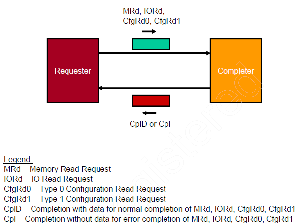
To explain the concept of outbound and inbound transactions, there are 2 entities that we need to keep in mind w.r.t the transactions that flow in the PCIe fabric:-
Initiator - component that initiates the transaction by sending a request. Example- Memory Read request sends the request for data.
Completer - component that receives the request and eventually sends a response. Example - After receiving Memory Read request sent by the initiator to it, it sends the completion TLP containing the requested data back to the initiator.

Transactions in PCIe can be categorized into 2 parts, depending on the direction of data flow relative to a device [Root complex or End-point] :-
Inbound - Data is coming into the device from the PCIe bus. From the device's perspective, the device is the completer of this request which was initiated by some other device. Example - Root complex[initiator] sending memory write TLP to an End-point[completer]. In this case EP will have inbound transactions coming from RC.
Outbound - Data is going out from the device to the PCIe bus. From the device's perspective, the device is the initiator of this request which will be completed by some other device. Example - End-point[Initiator] sending memory read TLP to a Root-complex[completer]. In this case, EP will have outbound transactions going towards RC.
What is ATU and why is it important in PCIe?
PCIe TLP transactions use PCIe addresses. These addresses are different from local internal bus addresses [like AXI, AHB] which are used in on-chip communication between CPU, memory and peripherals. So, we need an entity that maps the addresses from PCIe to local internal bus. Here comes the ATU: -
ATU is an Address Translation Unit that is responsible for address mapping between the device's address space and host's address space. It enables devices to access the host system's memory or other resources. Have a look at the following scenarios where ATU is needed: -
1. A PCIe device (such as network card, storage controller) needs to access the host's memory via DMA. So, the addresses that are issued by the device need to be translated via ATU so that the host can recognize and process these addresses.
2. A PCIe device wants to access a memory-mapped IO address. To do this, ATU is needed for translating device's requested address into an address that the host understands.
So, whenever a PCIe device initiates an access request like DMA memory read/write, the ATU translates the address issued by the device into the address of the host system as illustrated below: -
 ATU Translation
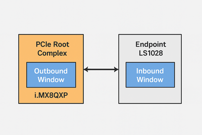
Now that we know what Inbound/Outbound transactions are and how does ATU work in PCIe, we will now discuss how to enable the devices [RC/EP] to carry out these transactions. To achieve this, we configure Inbound and Outbound windows in the PCIe controller of a device by setting up ATU translation.
How to configure PCIe Outbound and Inbound windows in iMX8QXP & LS1028 respectively?

For our use-case, we will be configuring 1 outbound window on iMX8QXP [Root Complex] and 1 Inbound window on LS1028A[Endpoint].
a. To set up an Outbound window on iMX8QXP, we configure the following registers:-
iATU Index register - defines which region is being accessed and its direction[Inbound/Outbound].
iATU Region Control 1 Register - To control some programmable bit fields
iATU Lower Base Address Register
&
iATU Upper Base Address Register
- These registers configure the start address of a window before the translation
iATU Limit Address Register - To configure the End-address of the window before the translation
iATU Lower Target Address Register
&
iATU Upper Target Address Register
- These registers configure the start and end addresses after the translation.
iATU Region Control 2 Register - To enable the REGION_EN bit and select match mode.
 Outbound Window
b. To set up an Inbound window on LS1028A, we configure the same set of registers :-
iATU Index Register
iATU Region Control 1 Register
iATU Lower Base Address Register
iATU Upper Base Address Register
iATU Limit Address Register
iATU Lower Target Address Register
iATU Upper Target Address Register
iATU Region Control 2 Register
Additionally, we will be configuring
PCI Express Command Register - to enable Bus master bit
PEX PF0 CONFIG Register - to set the Config Ready bit. Used by EP to indicate the RC that the controller has done its initialization.
The reason why we need to configure 2 additional registers on the EP side is that LS1028[EP] will be at Uboot console the whole time we are exercising our use-case. If it was in Linux, the PCIe drivers would have taken care of this.
 Inbound Window
Code-walkthrough
There's a patch attached with this blog so that the readers can go through it and use it if required.
Note:- In no way this claims itself to be a production level code, so readers are encouraged to only take it as a reference.
The Uboot patch achieves the following:-
- Configure MMU to make the DRAM range 80020000-88000000 non-cacheable. We are using the DRAM range 0x92000000-FE000000 as cacheable memory for our test case.
- Creates an outbound window on iMX8QXP[connected to LS1028 End-point via PCIe bridge]. To complement this, an Inbound window will be configured on the LS1028.
- In a loop:-
- zeroize the cacheable and non-cacheable 1MB memory region.
- flushing the data cache for the cacheable 1MB region.
- configure and trigger DMA read to transfer 1MB of data from End-point’s DDR to RC’s non-cacheable memory region.
- copy 1MB data from non-cacheable to cacheable memory.
- compares the cacheable 1MB memory with the expected data. If mismatch occurs, we error out and break out of loop. Otherwise the looping continues.
Executing ‘pci p’ command at U-boot console starts the above sequence.
After applying the patch in Uboot source, build the Uboot binary, then build SPL. Flash the SPL to iMX8QXP.
Running the test case
a. Connect RC [iMX8QXP] and EP[LS1028ARDB] via M.2 Key.E bridge, boot RC and EP till Uboot.
b. At Uboot console of LS1028, execute the following commands to configure the inbound window: -
mw.l 0x3500900 0x80000001
mw.l 0x3500904 0x0
mw.l 0x350090c 0x0
mw.l 0x3500910 0x0
mw.l 0x3500914 0x07ffff
mw.l 0x3500918 0xA0000000
mw.l 0x350091c 0x0
mw.l 0x3500908 0xC0000000
mw.b 0x3500004 0x06
mw.l 0x35C0014 0x00001001
The above registers are part of PCIe ATU configuration that was mentioned in the section -
How to configure PCIe Outbound and Inbound windows in iMX8QXP & LS1028 respectively
Please feel free to cross-check the Reference manual of LS1028A to verify the register addresses and their significance.
c. On RC, execute 'pci p' -- this will trigger the DMA transfer use-case.
This blog merely scratched the surface of PCIe inbound and outbound transactions. However it aimed at giving a raw view of how memory transfer can be triggered using DMA. For any queries, feel free to DM or send your questions in the comments section.
0001-pcie-dma-imx8qxprc-ls1028ep.patch
