- Forums
- Product Forums
- General Purpose MicrocontrollersGeneral Purpose Microcontrollers
- i.MX Forumsi.MX Forums
- QorIQ Processing PlatformsQorIQ Processing Platforms
- Identification and SecurityIdentification and Security
- Power ManagementPower Management
- Wireless ConnectivityWireless Connectivity
- RFID / NFCRFID / NFC
- Advanced AnalogAdvanced Analog
- MCX Microcontrollers
- S32G
- S32K
- S32V
- MPC5xxx
- Other NXP Products
- S12 / MagniV Microcontrollers
- Powertrain and Electrification Analog Drivers
- Sensors
- Vybrid Processors
- Digital Signal Controllers
- 8-bit Microcontrollers
- ColdFire/68K Microcontrollers and Processors
- PowerQUICC Processors
- OSBDM and TBDML
- S32M
-
- Solution Forums
- Software Forums
- MCUXpresso Software and ToolsMCUXpresso Software and Tools
- CodeWarriorCodeWarrior
- MQX Software SolutionsMQX Software Solutions
- Model-Based Design Toolbox (MBDT)Model-Based Design Toolbox (MBDT)
- FreeMASTER
- eIQ Machine Learning Software
- Embedded Software and Tools Clinic
- S32 SDK
- S32 Design Studio
- GUI Guider
- Zephyr Project
- Voice Technology
- Application Software Packs
- Secure Provisioning SDK (SPSDK)
- Processor Expert Software
-
- Cloud Lab Forums
- Topics
- Mobile Robotics - Drones and RoversMobile Robotics - Drones and Rovers
- NXP Training ContentNXP Training Content
- University ProgramsUniversity Programs
- Rapid IoT
- NXP Designs
- SafeAssure-Community
- OSS Security & Maintenance
- Using Our Community
-
-
- Knowledge Bases
- ARM Microcontrollers
- Identification and Security
- i.MX Processors
- Model-Based Design Toolbox (MBDT)
- QorIQ Processing Platforms
- S32 Automotive Processing Platform
- CodeWarrior
- Wireless Connectivity
- MCUXpresso Suite of Software and Tools
- MQX Software Solutions
- RFID / NFC
- Advanced Analog
-
- Home
- :
- NXP Tech Blog
- :
- Solving the Kinetis Debug Clock problem for Serial and CAN development
Solving the Kinetis Debug Clock problem for Serial and CAN development
Solving the Kinetis Debug Clock problem for Serial and CAN development
- Subscribe to RSS Feed
- Mark as New
- Mark as Read
- Bookmark
- Subscribe
- Printer Friendly Page
- Report Inappropriate Content
The internal clock frequency of Kinetis chips varies due to manufacturing tolerances. A trim value is programmed into the chips to compensate for this variance and make the slow bus frequency uniform between chips.
For some inexplicable reason, this trim value is not active during debug mode. This makes developing serial and CAN applications very difficult, as the baud rates which are set are not the baud rates which are achieved. To make matters worse, if I understand the documentation correctly, the baud rate in debug mode is different from the baud rate in normal mode.
I am working with KDS and USBDM which makes a beautiful IDE and works with processor expert. Unfortunately KDS is no longer under development and S32 does not support processor expert for my chips. Porting over to a newer development environment might help with the clock frequency issues, but with existing projects and code bases that is not an attractive solution. Perhaps some of these problems do not occur with commercial software or have been resolved in MCU Expresso and S32 design studio.
So, to fix this clock issue with KDS perform the following.
Load the trim value from memory you can control
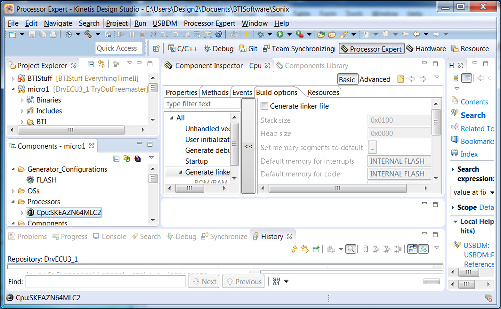
Figure 1: The processor expert tab with the processor selected
Go to the processor expert tab and click on your processor. In my case the processor is a SKEAZN64MLC2.
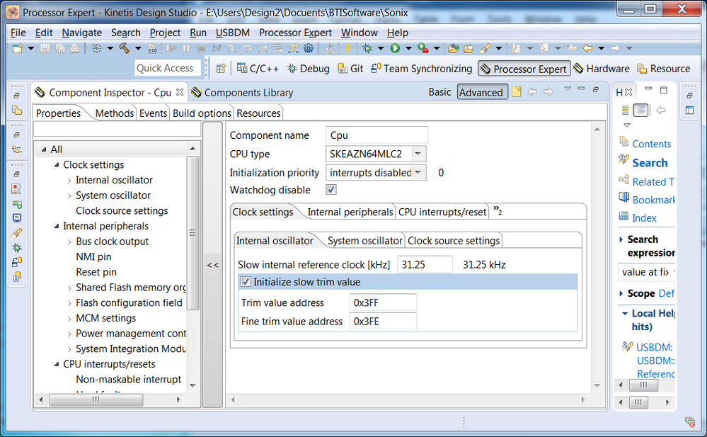
Figure 2: Adding code to initialize trim values from known memory locations
Maximize the component inspector so that you can see all the settings. Click on the Advanced tab, and put a check mark in the “Initialize slow trim value” box.
Clicking the “Initialize slow trim value” box writes the following code in the generated file CPU.c in order to load the trim value from addresses 0x3FE and 0x3FF.
if ( *((uint8_t*) 0x03FFU) != 0xFFU) {
ICS_C3 = *((uint8_t*) 0x03FFU);
ICS_C4 = (ICS_C4 & 0xFEU) | ((*((uint8_t*) 0x03FEU)) & 0x01U);
}
That part was easy.
Create linker memory description for locations 03FE and 03FF.
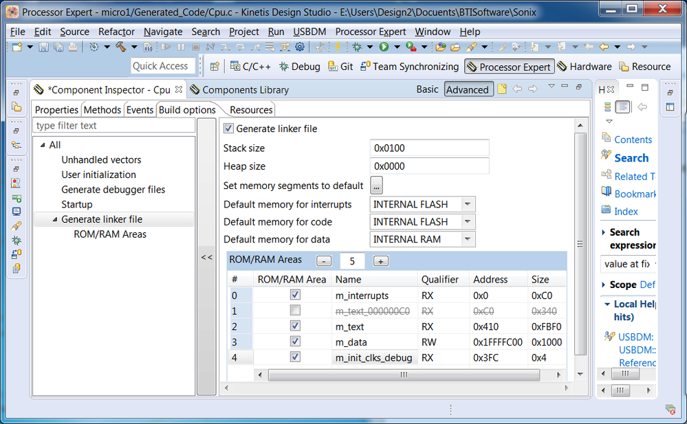
Figure 3: Adding a memory section for the values to be initialized.
Still in processor expert with your processor selected, go to the build options tab and select Generate linker file. If the check box for "Generate linker file" is not checked check it (after saving your linker file by checking it into git so that you can compare changes and restore any prior modifications). Add a Rom/Ram area by clicking on the “+” button—my new section is called “m_init_clks_debug”. Set the qualifier to RX so the linker knows it is for flash memory. Since memory is in 4 byte units on this chip, set it at address 0x3FC and make it 4 bytes long.
Adding the line to the ROM/RAM areas in the CPU component declares a memory location for a new section by adding the line
m_init_clks_debug (RX) : ORIGIN = 0x000003FC, LENGTH = 0x00000004
to the linker file ProcessorExpert.ld,
Initialize the memory locations.
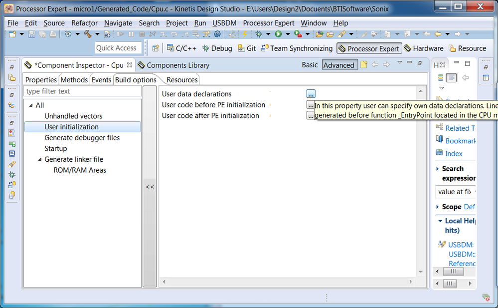
Figure 4: Initializing the memory location values.
Go to the Build-options tab and select the filter User initialization. Click the three dots next to User data declarations to brings up a dialog where data declaration code can be written. Fill in the dialog with
const __attribute__ ((section (".init_clks_debug"))) uint8_t dbg_clk_init[4] =
{
0x00,
0x00,
0x00,
0x9A
};
to create an array "dbg_clck_init[4]" in section ".init_clks_debug" and initialize its values in memory. The value 0x9A is the trim value, which will be unique for each chip.
Code written in the “User data declarations” dialog box is written in the beginning of the CPU.c file every time the component is regenerated. If you add the code manually to the CPU.c file, the code will be erased each time the file is regenerated.
Make the ".init_clks_debug" section in the linker file.
Figure 5: Editing the processor expert linker file
I have found no way to do this through processor expert, so generate your processor expert code to add all the changes made in the earlier steps into your generated c code. Then go back to the <Processor Expert> <Build Options><Generate linker file> tab (Figure 3) and un-check the “Generate linker file” check box. This will prevent further modification of your linker file, and allow you to create the necessary section manually.
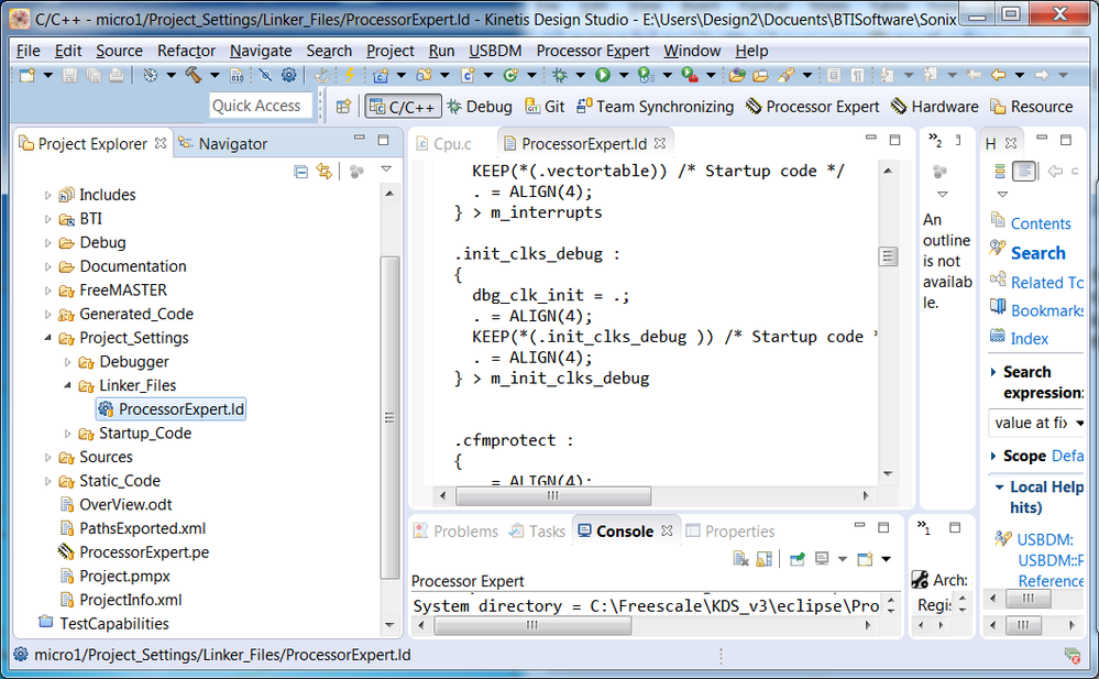
Open the linker file and add the following code to create the necessary section to put your initialized dbg_clk_init array into.
.init_clks_debug :
{
dbg_clk_init = .;
. = ALIGN(4);
KEEP(*(.init_clks_debug )) /* Startup code */
. = ALIGN(4);
} > m_init_clks_debug
Determine the proper trim value for your unique chip.
Figure 6: Finding the trim value
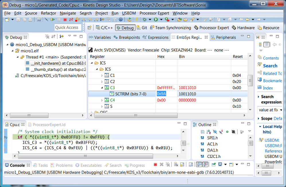
So far, it has worked for me to set a break point at the beginning of the code that was added to the Cpu.c file,
if ( *((uint8_t*) 0x03FFU) != 0xFFU) {
ICS_C3 = *((uint8_t*) 0x03FFU);
ICS_C4 = (ICS_C4 & 0xFEU) | ((*((uint8_t*) 0x03FEU)) & 0x01U);
}
and to inspect the ICS.C3 and ICS.C4 registers in the EmbSys Registers tab of the debug perspective as in figure 6.
This begs the question—why was all this necessary? Before doing this work the value showing in ICS.C3 was 0x80, which may be some default? This caused to set baud rate of 36000 to give an actual baud rate of 38400 on one chip, something different on another chip. Worse yet, according to the documentation the baud rate is not the same in debug mode and normal operating mode. After making these modifications and programming the proper trim value, the set baud rate matches actual baud rate that the serial or CAN bus uses.
A further benefit is that you can program a non-standard value to set a non-standard baud rate if there is a need. From the data sheet:
ICS_C3 is automatically loaded during reset from a factory programmed location when not in a debug
mode. The factory programmed trim value adjusts the internal oscillator frequency to fint_ft as specified in
the datasheet. The user can provide a custom trim value to attain other internal reference clock
frequencies within the fint_t range. The custom trim value must be programmed into reserved flash
location 0x0000_03FF and copied to ICS_C3 during code initialization.
Each increase in the ICS.C3 setting lowers the frequency of the intermediate clock bus by approximately 100 cycles per second.
You must be a registered user to add a comment. If you've already registered, sign in. Otherwise, register and sign in.
-
101
6 -
communication standards
8 -
General Purpose Microcontrollers
23 -
i.MX RT Processors
46 -
i.MX Processors
52 -
Interface
7 -
introduction
18 -
LPC Microcontrollers
73 -
MCUXpresso
35 -
MCUXpresso Secure Provisioning Tool
1 -
MCUXpresso Conig Tools
30 -
MCUXpresso IDE
43 -
MCUXpresso SDK
27 -
MCX
1 -
Model-Based Design Toolbox
6 -
MQX Software Solutions
2 -
PMIC
1 -
QorIQ Processing Platforms
1 -
QorIQ Devices
5 -
S32N Processors
4 -
S32Z|E Processors
6 -
SW | Downloads
8 -
日本語ブログ
13
- « Previous
- Next »
