- Forums
- Product Forums
- General Purpose MicrocontrollersGeneral Purpose Microcontrollers
- i.MX Forumsi.MX Forums
- QorIQ Processing PlatformsQorIQ Processing Platforms
- Identification and SecurityIdentification and Security
- Power ManagementPower Management
- Wireless ConnectivityWireless Connectivity
- RFID / NFCRFID / NFC
- Advanced AnalogAdvanced Analog
- MCX Microcontrollers
- S32G
- S32K
- S32V
- MPC5xxx
- Other NXP Products
- S12 / MagniV Microcontrollers
- Powertrain and Electrification Analog Drivers
- Sensors
- Vybrid Processors
- Digital Signal Controllers
- 8-bit Microcontrollers
- ColdFire/68K Microcontrollers and Processors
- PowerQUICC Processors
- OSBDM and TBDML
- S32M
- S32Z/E
-
- Solution Forums
- Software Forums
- MCUXpresso Software and ToolsMCUXpresso Software and Tools
- CodeWarriorCodeWarrior
- MQX Software SolutionsMQX Software Solutions
- Model-Based Design Toolbox (MBDT)Model-Based Design Toolbox (MBDT)
- FreeMASTER
- eIQ Machine Learning Software
- Embedded Software and Tools Clinic
- S32 SDK
- S32 Design Studio
- GUI Guider
- Zephyr Project
- Voice Technology
- Application Software Packs
- Secure Provisioning SDK (SPSDK)
- Processor Expert Software
- Generative AI & LLMs
-
- Topics
- Mobile Robotics - Drones and RoversMobile Robotics - Drones and Rovers
- NXP Training ContentNXP Training Content
- University ProgramsUniversity Programs
- Rapid IoT
- NXP Designs
- SafeAssure-Community
- OSS Security & Maintenance
- Using Our Community
-
- Cloud Lab Forums
-
- Knowledge Bases
- ARM Microcontrollers
- i.MX Processors
- Identification and Security
- Model-Based Design Toolbox (MBDT)
- QorIQ Processing Platforms
- S32 Automotive Processing Platform
- Wireless Connectivity
- CodeWarrior
- MCUXpresso Suite of Software and Tools
- MQX Software Solutions
- RFID / NFC
- Advanced Analog
-
- NXP Tech Blogs
- Home
- :
- モデルベース・デザイン・ツールボックス(MBDT)
- :
- モデルベース・デザイン・ツールボックス(MBDT)
- :
- Module 6: Current Sensing (Part 2/2)
Module 6: Current Sensing (Part 2/2)
- RSS フィードを購読する
- トピックを新着としてマーク
- トピックを既読としてマーク
- このトピックを現在のユーザーにフロートします
- ブックマーク
- 購読
- ミュート
- 印刷用ページ
Module 6: Current Sensing (Part 2/2)
- 新着としてマーク
- ブックマーク
- 購読
- ミュート
- RSS フィードを購読する
- ハイライト
- 印刷
- 不適切なコンテンツを報告
This is the part 2 of Module 6: Current Sensing (Part 1/2)
PDB Configuration
We finally reached to the most important part of the whole module. You may say that we "saved the best for last". This part make all the difference between reading the currents accurately or reading a total garbage. As a disclaimer, there is no bullet-proof method to setup the proper times for ADC reading. You will have to perform a series of tests that might be separated into 2 main categories:
- trial and error - start from an approximation of the known delays value and change the values steps by steps until you obtain the expected results;
- a combination of actual measurements and experiments to make sure the ADC sampling happens at the correct time intervals.
To demonstrate what i'm trying to say about these two methods let me share some oscilloscope captures with you that will prove my point. Now, i think is obvious for you why we have spent the time to implement the simple V/f open loop scalar control in Module 5: V/F Scalar Control . Having the possibility to drive the motor at various speeds allows us to investigate in detail how the current measurement works under real life conditions.
Lets start with Fig. 32, that shows the PDB interrupt triggered by the FTM PWM counter re-initialization. The interrupt is highlighted by a simple GPIO output pin toggle. Going further we have Fig. 33, that shows the phase A and B current variation. If we synchronize the PDB interrupt with the actual input to the ADC channel for one of the current and measure the waveform that corespondents to the worst case scenario as defined in Fig. 6, then we see that we might have up to 86us delay between the moment when the FTM is initialized and the moment when the lower transistor goes in conduction for the top speed we want to achieve. This is delay we want to consider for the PDB configuration.
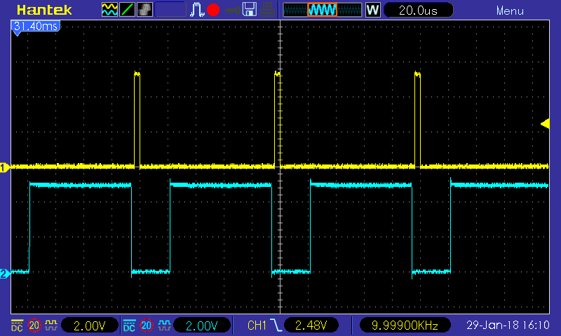 |
Fig. 32: Synchronization between PWM command for the lower switch (cyan) and PDB Interrupt (yellow) as result of FTM initialization trigger |
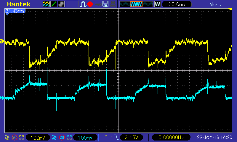 |
| Fig. 33: Phase A (yellow) and Phase B (cyan) voltage drop on the current shunt resistors |
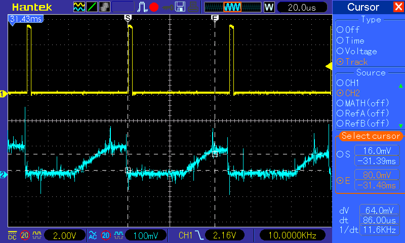 |
| Fig. 34: PDB interrupt (yellow) vs. phase current (cyan) at the highest speed we want to achieve. Note the 86us delay between FTM initialization trigger and the actual motor when the lower transistor goes in conduction |
Furthermore, if we check the DC-link shunt voltage drop that corresponds to the current that is drown from the power supply we can see its variation and the delay relative to the beginning of the PWM period. That is another information we want to consider for the PDB configuration.
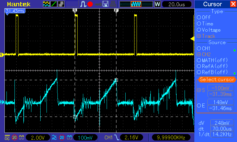 |
| Fig. 35: PDB interrupt (yellow) vs the DC-link current (cyan) at the highest speed we want to achieve. Note the 70us delay between FTM initialization trigger and peak of the DC-link current |
Based on the hardware measurement for the phase currents at high speeds and various experiments I've reached to the ADC triggering timings diagram shown in Fig. 36.
This diagram is valid for 10kHz PWM switching frequency only and shows how the ADC conversions are controlled via the PDB pre-triggers that are in turn delayed compared with the beginning of the PWM period. Please note that how the phase current ADC conversion are synchronized to happen in the same time for both ADC modules.
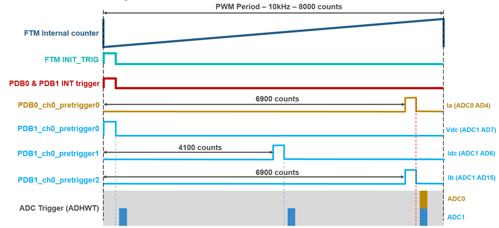 |
| Fig. 36: FTM-PDB-ADC triggering timings diagram |
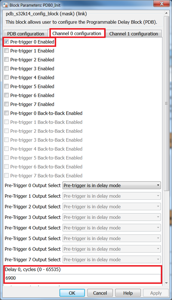
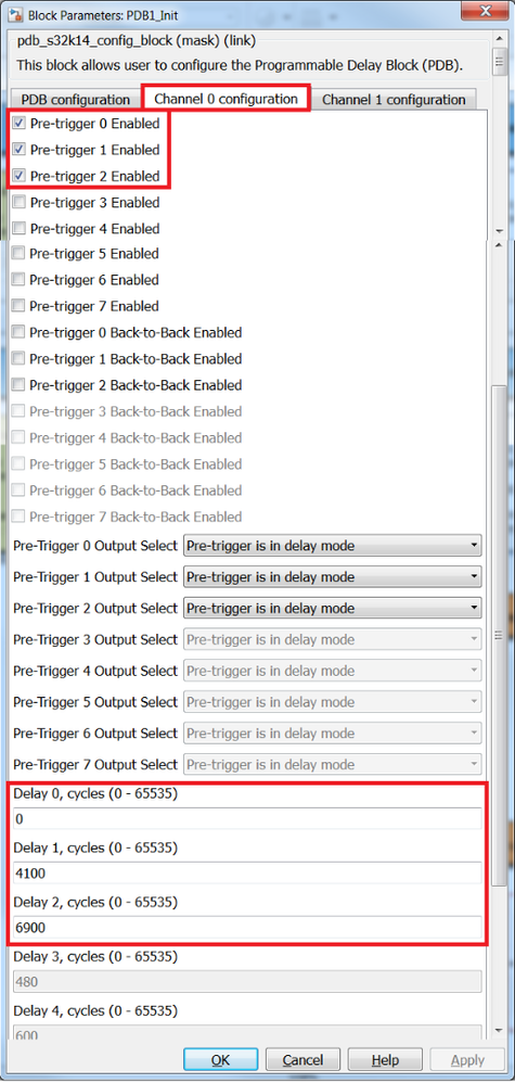
Based on the information shown in Fig. 36, we can configure the PDB0 and PDB1 instances directly from Simulink blocks
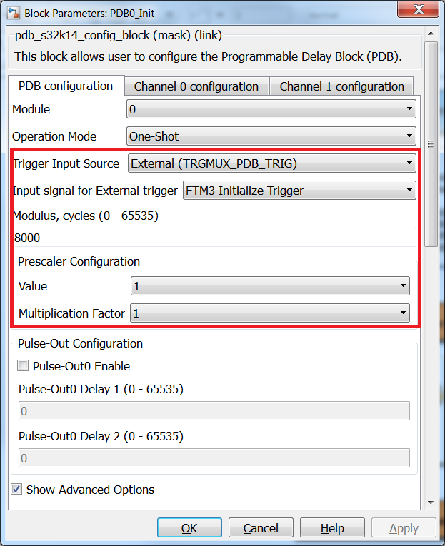 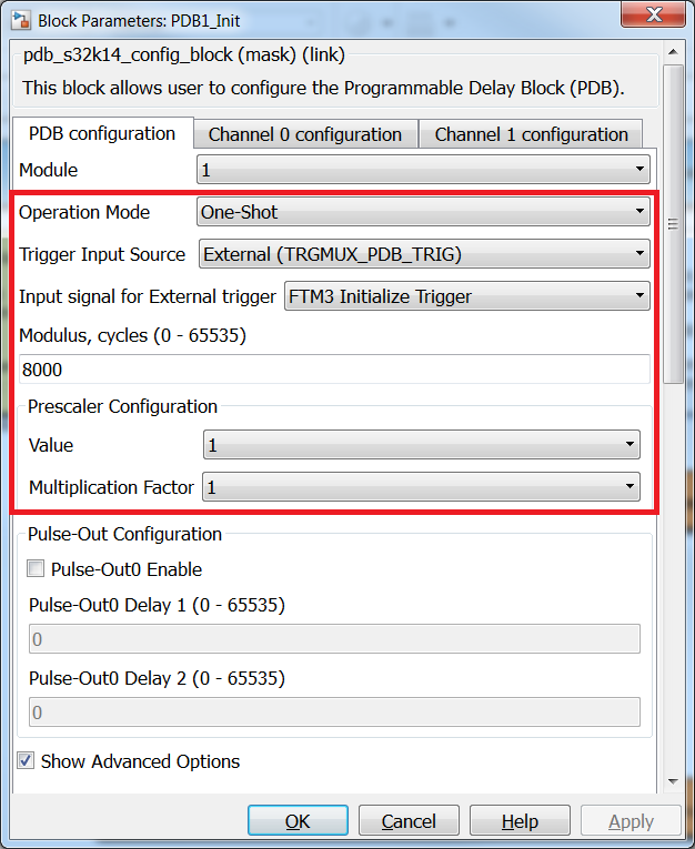 |
| Fig. 37: PDB0 and PDB1 global configurations: trigger source, external trigger type and PDB counter value |
| Fig. 38: PDB0 and PDB1 ADC pre-triggers and delays configuration with the timings shown in Fig.36 |
This way the PDB0 and PDB1 will trigger the ADC0 and ADC1 conversions at specific time intervals and all that remains for the CPU is to read those values and use them for FOC. To ADC0 and ADC1 conversion results are read on PDB1 interrupt handler that is triggered each time the PBD counter is re-initialized.
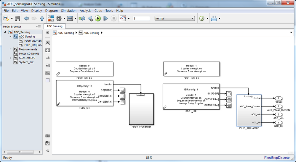 |
| Fig. 39: PDB0 and PDB1 interrupt configurations |
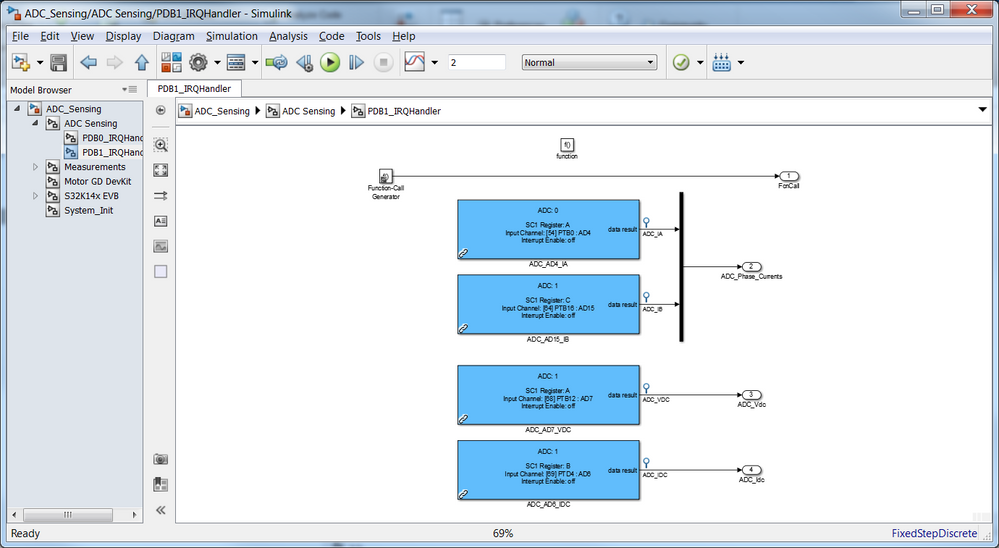 |
| Fig. 40: ADC conversion reading based on PDB interrupt |
For the moment the ADC conversion are read based on the PDB interrupt. This will be later on changed to read the values as soon as the last ADC hardware conversion is ready. This will ensure a minimal delay between the moment when the phase current are acquired and the moment when the next commutation sequence is updated.
For most of the common application that deals with relative small speed range this kind of mechanism is robust enough, but once you go into high speed regions like tens of thousandth of RPM the delay between the moment the current are measured and the computation of the rotor position is becoming critical. In practice to deal with such scenario you will need to perform electric angle compensation to avoid the lost of de-synchronization of PMSM.
MEASUREMENT OF CURRENTS and VOLTAGE
Once the ADC conversion are ready we need to transform those into actual currents and voltages by applying various scaling factors and offset compensation. We are not going crazy with explanations about how the ADC conversion works and how the read hardware implements the shunt voltage drop scaling. If you wish to get more information about this subject you may consult the Motor Control Class: Lecture 3 - Input Commands
The PMSM phase current measurement model is shown in Fig. 41. All you need to know is that the ADCs were configured to use 12bit precision and the shunts resistors can measure an instantaneous AC currents with the peak-to-peak amplitude of 31.25Amps
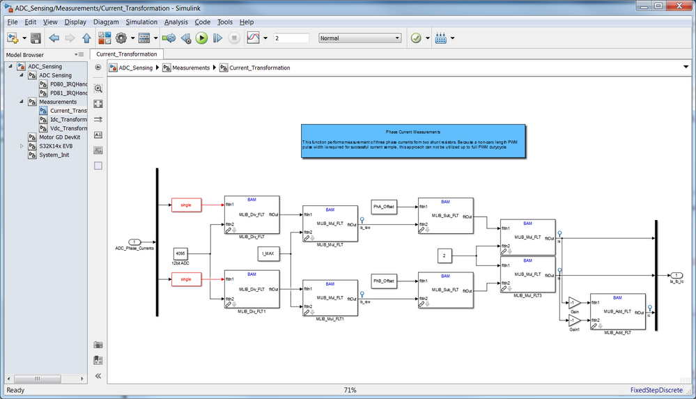 |
| Fig. 41: Phase current measurements - scaling and offsetting |
The DC-link bus voltage measurement Simulink model is shown in Fig. 42. Depending on the MotorGD DevKit jumper settings the DC voltage that can be measured via the voltage resistors divider network is up to 45Volts DC.
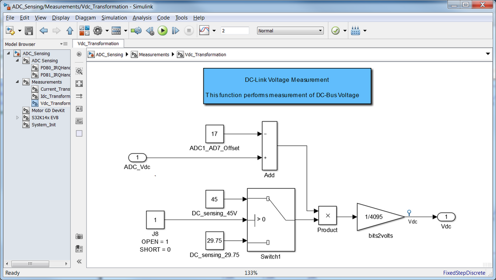 |
| Fig. 42: DC-link bus voltage measurement Simulink model |
And finally for the DC-link current the Simulink model used to covert the ADC acquisitions into actual Amps is shown in Fig. 43.
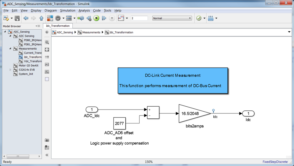 |
| Fig. 43: DC-link current measurement Simulink model |
EXPERIMENTAL RESULTS
If you reached to this point - then congratulations - it is now time to build the model and flash it into the MCU memory.
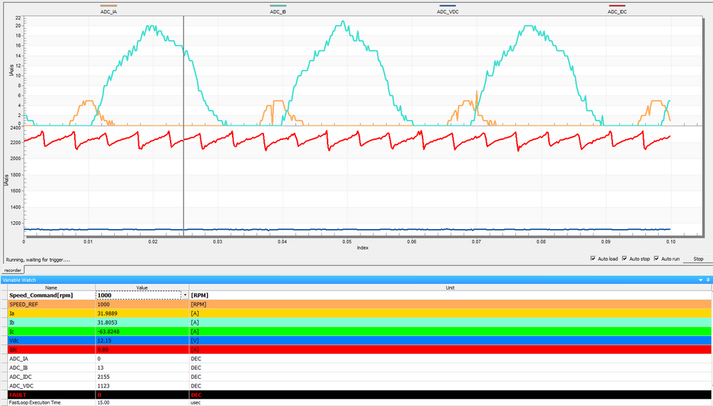
Using the FreeMASTER project attached ADC_Sensing.pmp we can visualize in real time the results of ADC conversions and validate the results.
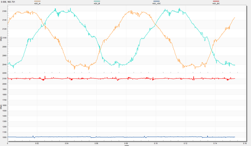 |
| Fig. 44: ADC conversion raw data: (yellow) - phase A current, (cyan) - phase B current, (red) - DC link current, (blue) - DC bus voltage |
 |
Fig. 45: 1000RPM PMSM phase currents: (yellow) - phase A current measured, (cyan) - phase B current measured, (green) - phase C current computed |
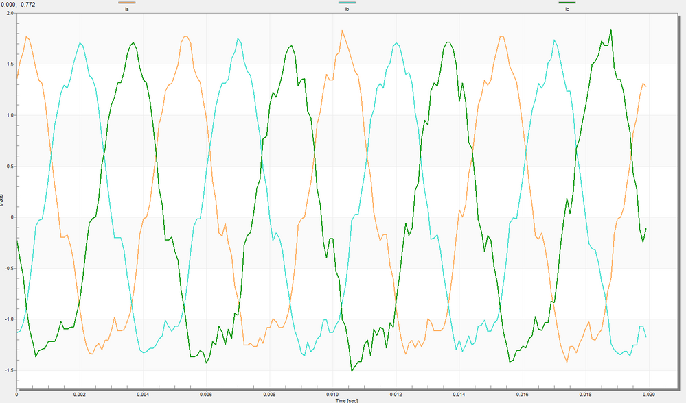 |
Fig. 46: 3000RPM PMSM phase currents: (yellow) - phase A current measured, (cyan) - phase B current measured, (green) - phase C current computed |
For DC bus values acquisitions we are going to modify the power supply voltage levels. The ADC acquisition from the target shall follow those variations.
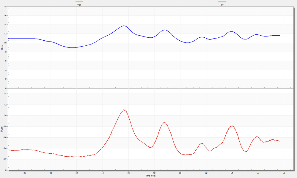 |
| Fig. 47: (blue) - DC bus voltage and (red) - DC bus current acquisitions |
Due to the scalar control method that keeps constant V/f ratio the DC-link current is going to follow the variations in the DC bus voltage.
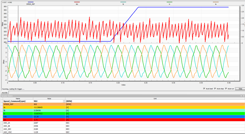
As a final validation we can check the PMSM startup sequence and how the values of the currents are changing over the time.
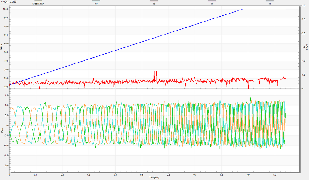 |
| Fig. 48: PMSM open loop V/f scalar control start-up sequence |
CONCLUSIONS
After going thru this module you should now have a good understanding about the hardware and software techniques required to perform various system measurements. You should now be aware of various tips & tricks to measure the most important quantities needed for Field Oriented Control. Depending on the hardware your are working on there might be slightly different hardware modules involved but the generic approach is the same: you need to synchronize the ADC readings with the PWM commands.
Another aspect that is highlighted in these 2 parts article is the correspondence between the actual analogue signals and the values used application. As you have seen the sensing information is totally different than what you normally expect as current waveform and it is up to the software to assemble all the pieces together and form the AC quantities we are all used with.
In the end I would like to highlight that each system engineer that is involved in the area of power drivers should always verify the measurements since those represent a very important factor in the overall control strategy. As you can see the measurements are polluted with EMI noise that may create us lot of problems later on. Understanding the rood cause of the noise and delay is a key factor towards a robust motor control solution.
Update January 28th 2019 - This Simulink model is now available on MATLAB 2018b and MBDT for S32K14x 2018.R1 release
Before using the new models make sure you apply all the hot-patches from here: HotFix: MBD Toolbox 2018.R1 for S32K
Update revisions:
March 18, 2019
- update the model to work with Model-Based Design Toolbox for MPC57xx Automotive Version 3.0.0 .
May 06, 2020
- update the model to work with Model-Based Design Toolbox for MPC57xx Automotive Version 3.2.0 .
- 新着としてマーク
- ブックマーク
- 購読
- ミュート
- RSS フィードを購読する
- ハイライト
- 印刷
- 不適切なコンテンツを報告
Hello dumitru-daniel.popa,
I downloaded the M6_2018.R1 file and i had to reroute the ADC Instance for current A from SE4 to SE2 because the SE4 instance is used by the LSPI Config Block and at 20 KHz PWM i got the following results
i tried the same procedure for 10 KHz with the same data that you used for PDB0 and PDB1 configurations but the motor didn't turn at all.
A second issue was with the torque Control model i did the same rerouting for Phase A but the board keeps going into the fault mode (Red LED).
Is there a way to avoid the LSPI block ? or did this rerouting caused the error with the torque Control?
Best Regards
Ali Terro
- 新着としてマーク
- ブックマーク
- 購読
- ミュート
- RSS フィードを購読する
- ハイライト
- 印刷
- 不適切なコンテンツを報告
Hi,
I want to use the hardware trigger of ADC for sample the CAN msg. The bit rate of CAN msg is 500Kbit/sec. When I set the options of the blocks PDB0_Init I choose as cycles 160 (ratio between 80MHz and 500KHz). It is possible to synchronize the ADC with the CAN with hardware trigger? I realized the communication on Model Based Design.
When I build my project I have this problem:
#if ( UCHAR_MAX != (0xFFU) ) || ( SCHAR_MAX != (0x7F) )
#error Code was generated for compiler with different sized uchar/char. \
Consider adjusting Test hardware word size settings on the \
Hardware Implementation pane to match your compiler word sizes as \
defined in limits.h of the compiler. Alternatively, you can \
select the Test hardware is the same as production hardware option and \
select the Enable portable word sizes option on the Code Generation > \
Verification pane for ERT based targets, which will disable the \
preprocessor word size checks.
#endif
Certainly I wrong Somethingand I need of help. Can someone help me?
Thanks
https://drive.google.com/file/d/1x5dUjxN9-x9FFXcp2AblMfNxMwZqBTB1/view?usp=sharing
https://drive.google.com/file/d/1GPFNSz14H9iEizeagQXPiuADF9A3ij5a/view?usp=sharing
- 新着としてマーク
- ブックマーク
- 購読
- ミュート
- RSS フィードを購読する
- ハイライト
- 印刷
- 不適切なコンテンツを報告
Hi dumitru-daniel.popa,
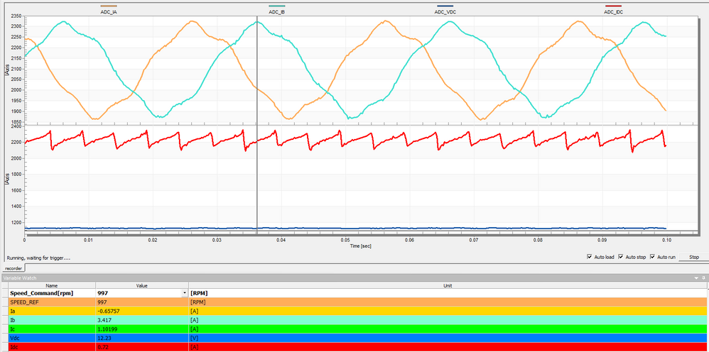
I am currently working with the MTRDEVKSBNK144 development kit, using MATLAB 2018b. I downloaded M6_2018.R1.zip and I had it uploaded on S32. I did apply the Cumulative Patch found in the HotFix thread beforehand (The "Replace All" message appeared) .
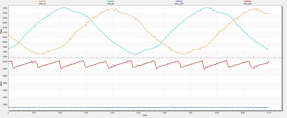
Unfortunately, I cannot succeed in making it do the right thing. I posted below my FreeMaster results
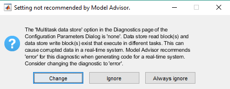
(This warning comes out every time I build the model, but I don't think this is the cause)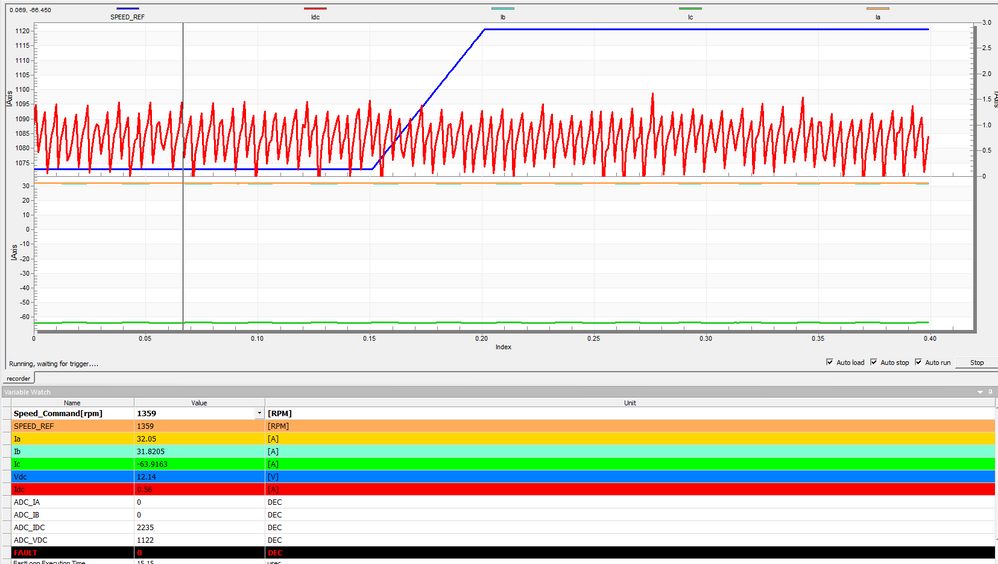
Ia, Ib and Ic are supposed to be sine waves.
Regarding the picture containing the ADC_IB and ADC_IB, the phase shift seems good, but the amplitude of ADC_IA is too low. Also, isn't the ADC_IDC shape odd?
Thank you in advance.
Best regards,
Andrei Cador
- 新着としてマーク
- ブックマーク
- 購読
- ミュート
- RSS フィードを購読する
- ハイライト
- 印刷
- 不適切なコンテンツを報告
Indeed the current reading are wrong.
Have you set the MTRDEVKSBNK144 to operate in the PMSM mode (J11/J10/J09)?
Are you absolutely sure you have installed:
- Toolbox: https://community.nxp.com/docs/DOC-341052
- Patch: https://community.nxp.com/thread/489947#comment-1106251
The text and the screenshots from the article was written for a slightly older toolbox. In the latest toolbox we have changed a bit the UIs. The models with *_2018.R1* were tested and validated before being uploaded here.
Best regards,
Daniel
- 新着としてマーク
- ブックマーク
- 購読
- ミュート
- RSS フィードを購読する
- ハイライト
- 印刷
- 不適切なコンテンツを報告
Thank you very much for your fast response, dumitru-daniel.popa.
Seems like I did not change those jumpers for PMSM operating mode. I thought it was the default mode and I did not go through that part of the guide.
I wish to add one more question to be sure that my motor is functioning the way it should.
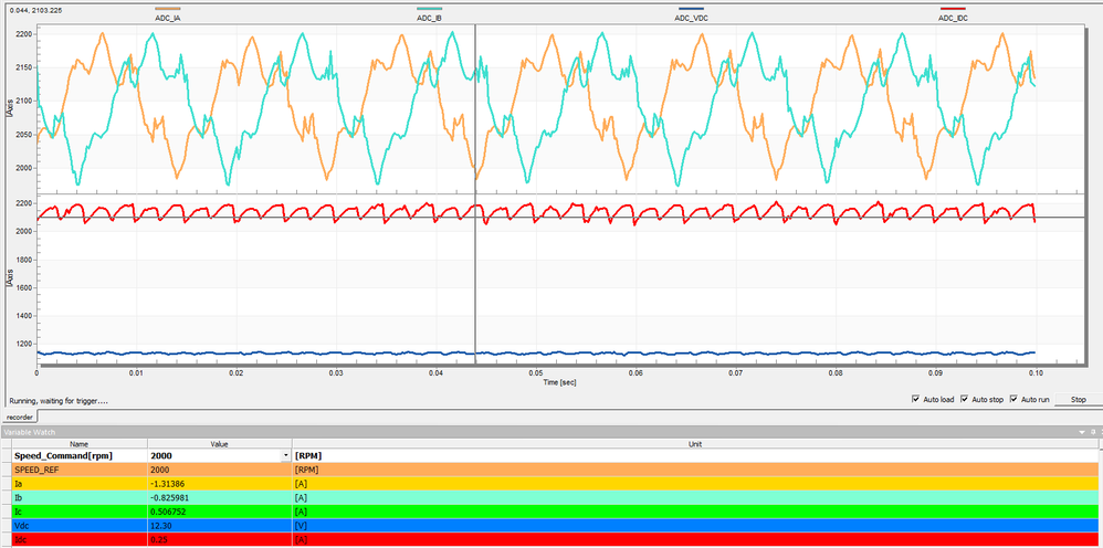
Are the measurements for 2000RPM regime too noisy? I think it's important to mention that 2000RPM is the biggest value I can set, providing the fact that Fig. 46 showed 3000 RPM.
Thank you in advance.
Best regards,
Andrei Cador
- 新着としてマーク
- ブックマーク
- 購読
- ミュート
- RSS フィードを購読する
- ハイライト
- 印刷
- 不適切なコンテンツを報告
The motor which is part of the kit is a BLDC motor (the back-emf waveform is square). Also, keep in mind that the motor max speed is 4000 rpm @ 24V. The DC bus voltage used on the kit is only 12Vdc hence you can't drive the motor stable for more than 2000rpm.
These are some aspects that you need to consider when you drive this default motor. If you have a change to change the motor with a more reliable 12V motor with sine back emf waveform, then please do it - the quality if the currents will be drastically improved.
Hope this helps!
Daniel
- 新着としてマーク
- ブックマーク
- 購読
- ミュート
- RSS フィードを購読する
- ハイライト
- 印刷
- 不適切なコンテンツを報告
Thank you very much for explanation, it does help a lot (si proiectul meu de licenta va multumeste).
Have a nice day,
Andrei Cador
- 新着としてマーク
- ブックマーク
- 購読
- ミュート
- RSS フィードを購読する
- ハイライト
- 印刷
- 不適切なコンテンツを報告
Hi,
I use MTRDEVKSBNK144 Application Software.
I have a question about the application code.
1. For sensing the DC link voltage, DC link current, Phase voltage,
PDB_DRV_SetTimerModulusValue (INST_PDLY0, HALF_PWM_MODULO);
Is there any reason to set 2000 to 4000 instead of Full PWM?
When setting to HALF_PWM, I want to know if AD conversion is possible for 0 ~ 2000 and AD conversion is not possible for 2000 ~ 4000.
2. At present, the information of other sensors is required, so it is necessary to add about 4 channel ADC.
Therefore, the PDB delay must be add in AD sequence.
I want to know the minimum PDB delay time for other AD conversions after one AD conversion in PDB_DRV_SetAdcPreTriggerDelayValue().
3. Is there any other way not to add PDB delays?
For example, a continuous ADC.
Thanks you.
- 新着としてマーク
- ブックマーク
- 購読
- ミュート
- RSS フィードを購読する
- ハイライト
- 印刷
- 不適切なコンテンツを報告
Hi sohyunjang,
I might not be the best person to answer these questions - but for the sake of convenience since the topics are somehow related with the subject of this article - i'm going to give it a try.
1. For sensing the DC link voltage, DC link current, Phase voltage,
PDB_DRV_SetTimerModulusValue (INST_PDLY0, HALF_PWM_MODULO);
Is there any reason to set 2000 to 4000 instead of Full PWM?
When setting to HALF_PWM, I want to know if AD conversion is possible for 0 ~ 2000 and AD conversion is not possible for 2000 ~ 4000.
The SW you are using is a reference design from NXP and if you check the fast control loop execution you will see that the current measurements are performed at every other second PWM update.
The FTM3 PWM module which triggers a whole “chain” of peripheral blocks FTM3_initialization->PDB0/1->ADC0/1 has an operating frequency of 20 kHz (you want to have the PWM as high as possible to eliminate audible noise and limit the EMI)
Since in Sensorless mode you need to perform a lot of computations in the fast control loop (10kHz) - which is in sync with the ADC measurements - you need to make sure you have enough time to finish you computation before being interrupted by other tasks (slow loop, data aquisition, etc) that also need to be executed.
Therefore, NXP has employed a trick - skips one PWM update interrupt and measure the ADC signals at every second one.
In addition there are 2 other aspects we need to count for:
- the motor phase currents are read with shunts resistors that are mounted in the lower part of the inverter
- the PWM signals are generated based on center-aligned method
These 2 aspects ensure that in the middle of the PWM (2000) out of full PWM (4000) we will find the lower transistor in conduction and we will be able to measure the motor phase current.
Since the PBD is triggered at every other second PWM initialization event, then the PDB counter is set to count only till the half of the PWM period.
Of course you can measure values like DC bus voltage at any point between 0-4000 but the phase current can only be acquired in a specific points when using shunt resistors in lower inverter legs.
2. At present, the information of other sensors is required, so it is necessary to add about 4 channel ADC.
Therefore, the PDB delay must be add in AD sequence.
I want to know the minimum PDB delay time for other AD conversions after one AD conversion in PDB_DRV_SetAdcPreTriggerDelayValue().
There is no problem in adding additional ADC triggered conversions. Now the delay depends on your particular system. You can see my analysis here: Module 6: Current Sensing (Part 1/2)
For the beginning you can start by adding a 200-300 range PDB delay for each of the triggered ADC conversion.
Keep in mind that you can also tweak the ADC settings in order to make if faster but will consume more power.
3. Is there any other way not to add PDB delays?
For example, a continuous ADC.
If you wish to have a chain of events between the PWM-PDB-ADC i think that might be the only feasible way to go forward. In the end that is why Programmable - Delay - Block was invented :-)
Anyhow - you might trigger jobs execution based on a various trigger events but that means a lot of overhead in SW. I think the best thing here is to stick with PDB, understand your HW design delays (eventually measure those with an oscilloscope) and offload all these chaining events from CPU to the dedicated peripherals.
Hope this helps!
Daniel
- 新着としてマーク
- ブックマーク
- 購読
- ミュート
- RSS フィードを購読する
- ハイライト
- 印刷
- 不適切なコンテンツを報告
The PMSM phase current measurement model is shown in Fig. 41. All you need to know is that the ADCs were configured to use 12bit precision and the shunts resistors can measure an instantaneous AC currents with the peak-to-peak amplitude of 31.25Amps
Where did you found this Information of 31.25 Peak-to-Peak Amplitude ?
For the Motor GD Kit I only found 5A phase current (RMS) in the overview.
I didn't found a schematic.
- 新着としてマーク
- ブックマーク
- 購読
- ミュート
- RSS フィードを購読する
- ハイライト
- 印刷
- 不適切なコンテンツを報告
Hi Leon,
Indeed, the schematics of the MotorGD DevKit are not yet available on the website. I've made a note to NXP persons responsible for uploading the documentation. I do not have a public approved version therefore i can't share it here.
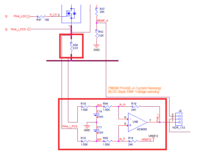
What i can share is how the current measurement is implemented. PHA_I goes directly on MCU ADC pin just like the other signals for the B and C phase currents.
I'm not an electronic engineer, but apparently if you do the math, that's the theoretical range.
Hope this helps!
Daniel
- 新着としてマーク
- ブックマーク
- 購読
- ミュート
- RSS フィードを購読する
- ハイライト
- 印刷
- 不適切なコンテンツを報告
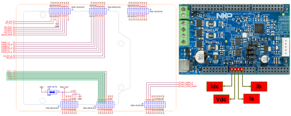
thank you for the image. If I'm correct the J9 is connected between pin 1 and 2.
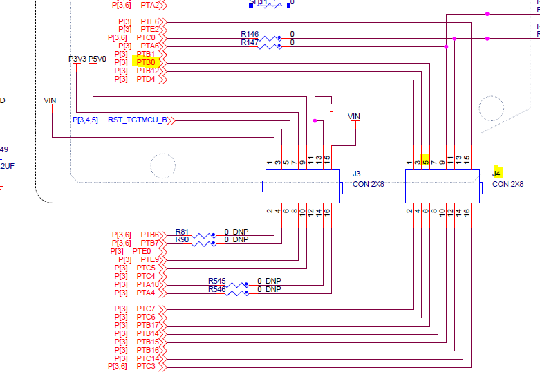
Then J9 pin 2 should be connected with J4 Pin 5 in the image below ?
Motor GD
S32K
J4 Pin 5 is then connected on s32k PTB0
PTB0 you have configured in the adc block.
If this is correct then the + terminal of the Operation amplifier is connected to the upper side of the shunt (PHA_I_POS) while the - terminal is connected to the lower side of the shunt.
Here is a difference to the High Voltage Development Platform !
MC3PH
Here the + terminal of the Operation amplifier for current measurements is connected to the lower side of the shunt while the - terminal is connected to the upper side.
So with MC3PH here the Inversion of the sign is already done and I do not need to consider this in Software?
The note in the schematic "1.65V +/- 1.65V @ +/- Imax" would be okay !
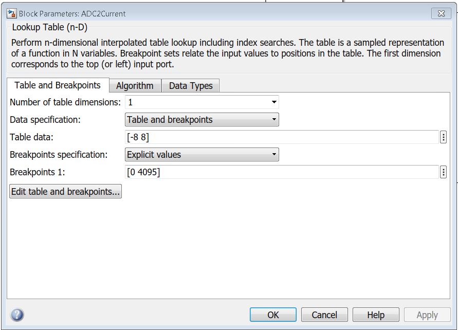
On the Basis of my previous model for measuring the currents I have configured a LUT like this:
Best regards
Leon
