- Forums
- Product Forums
- General Purpose MicrocontrollersGeneral Purpose Microcontrollers
- i.MX Forumsi.MX Forums
- QorIQ Processing PlatformsQorIQ Processing Platforms
- Identification and SecurityIdentification and Security
- Power ManagementPower Management
- Wireless ConnectivityWireless Connectivity
- RFID / NFCRFID / NFC
- Advanced AnalogAdvanced Analog
- MCX Microcontrollers
- S32G
- S32K
- S32V
- MPC5xxx
- Other NXP Products
- S12 / MagniV Microcontrollers
- Powertrain and Electrification Analog Drivers
- Sensors
- Vybrid Processors
- Digital Signal Controllers
- 8-bit Microcontrollers
- ColdFire/68K Microcontrollers and Processors
- PowerQUICC Processors
- OSBDM and TBDML
- S32M
- S32Z/E
-
- Solution Forums
- Software Forums
- MCUXpresso Software and ToolsMCUXpresso Software and Tools
- CodeWarriorCodeWarrior
- MQX Software SolutionsMQX Software Solutions
- Model-Based Design Toolbox (MBDT)Model-Based Design Toolbox (MBDT)
- FreeMASTER
- eIQ Machine Learning Software
- Embedded Software and Tools Clinic
- S32 SDK
- S32 Design Studio
- GUI Guider
- Zephyr Project
- Voice Technology
- Application Software Packs
- Secure Provisioning SDK (SPSDK)
- Processor Expert Software
- Generative AI & LLMs
-
- Topics
- Mobile Robotics - Drones and RoversMobile Robotics - Drones and Rovers
- NXP Training ContentNXP Training Content
- University ProgramsUniversity Programs
- Rapid IoT
- NXP Designs
- SafeAssure-Community
- OSS Security & Maintenance
- Using Our Community
-
- Cloud Lab Forums
-
- Knowledge Bases
- ARM Microcontrollers
- i.MX Processors
- Identification and Security
- Model-Based Design Toolbox (MBDT)
- QorIQ Processing Platforms
- S32 Automotive Processing Platform
- Wireless Connectivity
- CodeWarrior
- MCUXpresso Suite of Software and Tools
- MQX Software Solutions
- RFID / NFC
- Advanced Analog
-
- NXP Tech Blogs
- Home
- :
- General Purpose Microcontrollers
- :
- Kinetis Microcontrollers
- :
- Re: What's the minimum circuit requirement for KL/K mcu programming?
What's the minimum circuit requirement for KL/K mcu programming?
- Subscribe to RSS Feed
- Mark Topic as New
- Mark Topic as Read
- Float this Topic for Current User
- Bookmark
- Subscribe
- Mute
- Printer Friendly Page
- Mark as New
- Bookmark
- Subscribe
- Mute
- Subscribe to RSS Feed
- Permalink
- Report Inappropriate Content
I am trying my best to use FRDM on board OpenSDA debugger to program hex/srec/bin code into off-board KL25Z/K20 boards.
I got the following errors:
- Keil + CMSIS-DAP firmware, SWD/JTAG communication error
- IAR + PEmicro OpenSDA firmware, a setup window popup to show no target MCU found.
- Coocox + CoLinkEX + CoFlash, "Flash not blank !!! -> Can NOT Stop MCU !!!"
SWD should be the simplest way to program a cortex micro. (VCC/GND, DIO/CLK/RST) I have double checked the connections. They are good.
But I have changed a TXC 8MHz crystal in these boards. I want to know if the crystal can influence the SWD programming? Is it possible to program a bare KL25Z chip (only MCU mounted on board, not crystal, only SWD connections are available, and power source comes from SWD as well) ?
So far I don't think cystal issue is the root cause of programming failure, because KL25Z can run from IRC. FSL can not enforce customer to add crystal for programming.
It is surprise to me when I failed in programming KL25Z with FRDM+CMSIS-DAP. This CMSIS-DAP programming configuration is even working well for other MCU.
Solved! Go to Solution.
- Mark as New
- Bookmark
- Subscribe
- Mute
- Subscribe to RSS Feed
- Permalink
- Report Inappropriate Content
I added a series resistor on SWD_CLK, then most of debuggers can talk to KL25Z.
- MultiLink (Passed)
- PEmicro for OpenSDA/FRDM (Failed, because its driver is overwritten by Multilink?)
- JLINK for OpenSDA/FRDM (Passed)
- CMSIS-DAP for OpenSDA/FRDM (Passed)
- USBDM for OpenSDA/FRDM (Passed)
- CooCox CoLinkEX (Failed, check cable)
Some FAE told me that is impedance matching. I don't know, 1MHz SWD clk requires impedance matching circuit? I used to think only 100MHz + requires impedance matching.
Anyway, we can close this issue now.
Well, let me thank people who have helped me out of that.
pgo, thanks for point me to right direction, from silicon to my board. I hope it doesn't bug you too much.
speer & Gary Guo, thanks for assign FAE to help me.
Mr. Wang Peng, thanks for your profesional services and precious time to replace damaged samples on board and offer me more samples to test. and tell me the hardware design principles.
FAE ConstYu, thanks your comments on Chinese FSL community, for adding resistor on CLK.
FuMing, my friend, thanks for allowing me to use your debugger.
Yours sincerely
Allan K Liu
- Mark as New
- Bookmark
- Subscribe
- Mute
- Subscribe to RSS Feed
- Permalink
- Report Inappropriate Content
How big is this series resistor?
- Mark as New
- Bookmark
- Subscribe
- Mute
- Subscribe to RSS Feed
- Permalink
- Report Inappropriate Content
220R is enough.
- Mark as New
- Bookmark
- Subscribe
- Mute
- Subscribe to RSS Feed
- Permalink
- Report Inappropriate Content
Hi, same problem on my board. I have a voltage of 1.5V on the reset pin with usbdm programmer. Tomorrow i will read the pin with an oscilloscope and try your solution. I have tried three different kl25 and all with the same problem.
- Mark as New
- Bookmark
- Subscribe
- Mute
- Subscribe to RSS Feed
- Permalink
- Report Inappropriate Content
Hi Daniele,
What USBDM programmer are you using?
bye
- Mark as New
- Bookmark
- Subscribe
- Mute
- Subscribe to RSS Feed
- Permalink
- Report Inappropriate Content
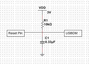
I'm using USBDM like here Using the Freedom Board as SWD Programmer | MCU on Eclipse. I have tried different solution but the problem still.
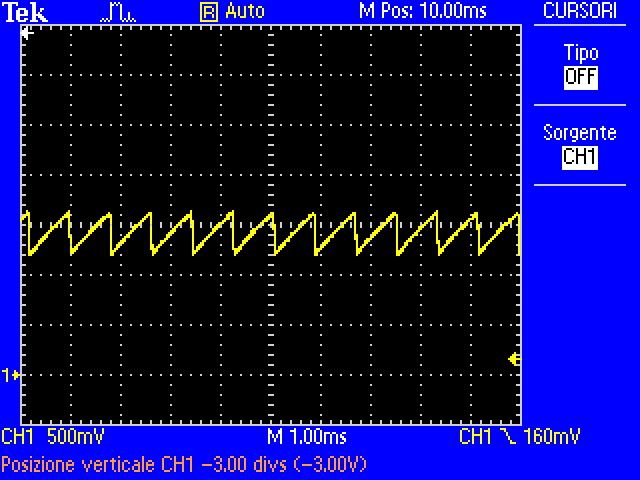
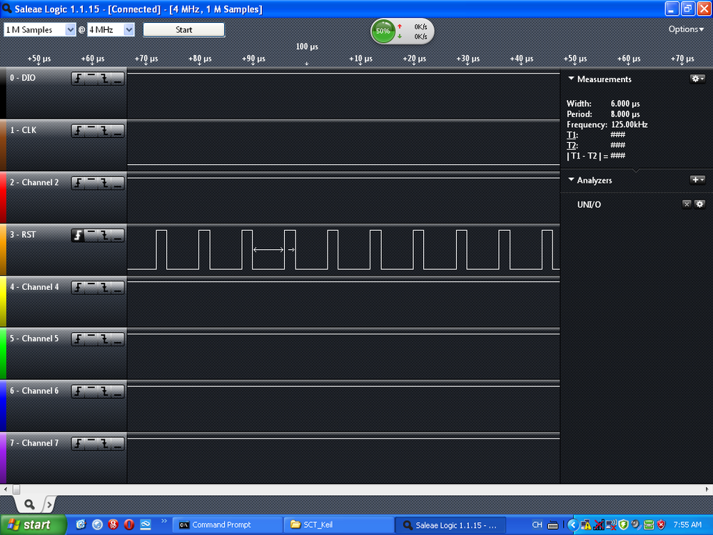
This is the signal that i read on the reset pin with this circuit
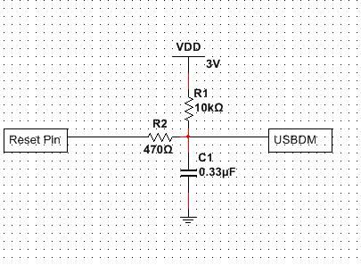
if i add this resistence of 470R
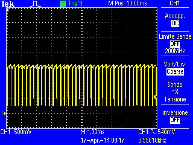
i see this signal on the reset pin
the problem is that the signal is only 1.5V, then i can't program the micro. I don't understand why the kl25 continue to reset ....
- Mark as New
- Bookmark
- Subscribe
- Mute
- Subscribe to RSS Feed
- Permalink
- Report Inappropriate Content
Hi Daniele,
Does the programmer work OK with the on-board KL25 chip?
Also make sure you have programmed a dummy program to the on-board chip before using the external programmer. See at the bottom of this page:
USBDM: Setting Up the FRDM-KL25Z
The waveform you are seeing is to be expected from a blank chip. The target device will be resetting itself due to either a watchdog timer expiration or due to executing an illegal instruction. I've never bothered determining which.
This should not interfere with the programming. I have confirmed this with a few different chips.
Does the stand-alone programmer detect the device at all?
Also selecting mass erase will usually be more reliable.
bye
- Mark as New
- Bookmark
- Subscribe
- Mute
- Subscribe to RSS Feed
- Permalink
- Report Inappropriate Content
I'm using a frdm kl05 instead kl25, the programmer didn't have problem. I have two same boards, with one i didn't have problem but with this yes.
- Mark as New
- Bookmark
- Subscribe
- Mute
- Subscribe to RSS Feed
- Permalink
- Report Inappropriate Content
I added a series resistor on SWD_CLK, then most of debuggers can talk to KL25Z.
- MultiLink (Passed)
- PEmicro for OpenSDA/FRDM (Failed, because its driver is overwritten by Multilink?)
- JLINK for OpenSDA/FRDM (Passed)
- CMSIS-DAP for OpenSDA/FRDM (Passed)
- USBDM for OpenSDA/FRDM (Passed)
- CooCox CoLinkEX (Failed, check cable)
Some FAE told me that is impedance matching. I don't know, 1MHz SWD clk requires impedance matching circuit? I used to think only 100MHz + requires impedance matching.
Anyway, we can close this issue now.
Well, let me thank people who have helped me out of that.
pgo, thanks for point me to right direction, from silicon to my board. I hope it doesn't bug you too much.
speer & Gary Guo, thanks for assign FAE to help me.
Mr. Wang Peng, thanks for your profesional services and precious time to replace damaged samples on board and offer me more samples to test. and tell me the hardware design principles.
FAE ConstYu, thanks your comments on Chinese FSL community, for adding resistor on CLK.
FuMing, my friend, thanks for allowing me to use your debugger.
Yours sincerely
Allan K Liu
- Mark as New
- Bookmark
- Subscribe
- Mute
- Subscribe to RSS Feed
- Permalink
- Report Inappropriate Content
Well. I would like to update for this issue.
As pgo said, 125KHz output is normal in new sample. I visited FSL Shanghai this morning and met Mr. Peng Wang in the office. Up to now, we can draw some conclusions and some speculates so far.
Fact 1: None of these boards can be connected to most of the debugger. (Speculate: They may have been damaged during POR, due to improper PCB layout, like long and narrow GND and long trace for reset which may introduces too much noise )
Fact 2: By adding more decoupling capacitor and replacing with a new KL25Z, it talks to JLINK (clone) in command mode (The new KL25Z can be detected with following info with a script from Mr. Wang:
Reset delay: 0 ms
Reset type RESETPIN: Resets core & peripherals using RESET pin.
Info: Found SWD-DP with ID 0x0BC11477
Info: FPUnit: 2 code (BP) slots and 0 literal slots
Info: Found Cortex-M0 r0p0, Little endian.

R0 = 00000023, R1 = 1FFFF410, R2 = 00000000, R3 = 00000000
R4 = 00000000, R5 = 00000000, R6 = 00000000, R7 = 00000000
R8 = 002001B0, R9 = 01489800, R10= 886084A0, R11= 04420B2C
R12= 840982DF, R13= FFFFFFFC, MSP= FFFFFFFC, PSP= 33012A20
R14(LR) = 00000A1D, R15(PC) = FFFFFFFE
XPSR 81000000, APSR 80000000, EPSR 01000000, IPSR 00000000
CFBP 00000000, CONTROL 00, FAULTMASK 00, BASEPRI 00, PRIMASK 00
Fact 3: However, it still can not talk to other debugger, including OpenSDA/CMSIS-DAP/CoLinkEx in SWD mode. As a cross checking, these debugger can program on board KL25Z of FRDM-KL25Z.
Fact 4: Although JLINK is the only one which can talk with KL25Z, but it refused to work because it is a clone.
We don't have enough time to arrange an inspection over the circuit with oscilloscope.
From viewpoint of schematics, it is working. But I have to revise the PCB with proper GND, shorter SWD connections.
However, I still have no idea how to debug it, or even download the code. Does JLINK commander support code programming?
- Mark as New
- Bookmark
- Subscribe
- Mute
- Subscribe to RSS Feed
- Permalink
- Report Inappropriate Content
Now I found there is 125KHz signal comes from reset pin, check thread on https://community.freescale.com/message/384630#384630
Now I found it, but I have no idea how to solve it.
- Mark as New
- Bookmark
- Subscribe
- Mute
- Subscribe to RSS Feed
- Permalink
- Report Inappropriate Content
I tested again for programming my custom KL25Z boardwith OpenSDA of FRDM-KL25Z. Still fails on SWD communication error.
Debug Proble
I am not good at hardware debugging so I list my checklist here.
Cross checking with Cortex-M0+ mini board with LPC812 (NXP), success.
Cross checking with Cortex-M0+ mini board with LPC811 (NXP), success.
Cross checking with Crotex-M0 mini board with LPC1114F (NXP), success.
OpenSDA with KL25Z, fails (communication error).
Conclusion: board issues caused by KL25Z, OpenSDA works well.
Power supply
Check power supply, 3.3V regulated. (both from OpenSDA 3.3V pin headers as well as LDO from KL25Z board)
Check ground, done.
Decoupling caps, soldered. done.
Conclusion: Very good power supply with common ground.
Cables
Wire connection (RST/DIO/CLK), good, less than 10 Ohm (using IDC cable as well as other shorter wires as cross checking)
Power up measurement
VCC:3V, RST:3V, DIO:3V, CLK:3V (NXP board)
VCC:3V, RST:1.5V, DIO:0V, CLK:0V (KL25Z)
Reset Circuit?
It seems RST is not stable or keep MCU in reset state. I checked my schematics & PCB layout.
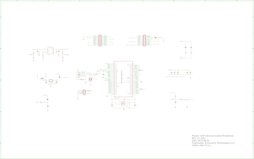
Shematics (EAGLE)
The reset of SWD connects to MCU, and push button with 10K weak pull-up and 1uF to ground. (Although 1uF cap to GND looks big, but it is same as FRDM.)
In fact, I also tested (not fully tests) on a bare PCB with only SWD sockets and MCU on board. The reset connection from SWD to MCU is short enough, and 10K pull-up and 1uF to GND are empty. The reset should be fully under control of OpenSDA. Why this happens again?
In my last attempt programming with CoLinkEx, which use buffer IC to drive reset as well. It will reports "CAN NOT STOP MCU". Is there anything I should take care of reset?
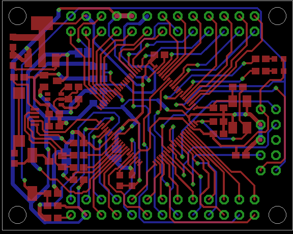
PCB (EAGLE)
The PCB routing looks bad, it almost route three corners of the whole board. You can identify the right side SWD socket, the most right down corner is reset, then you can find the reset net links to reset pad, the other branch goes up, goes left most, before goes down to push button and 10K resistor and 1uF cap.
So far I can only find this "suspicious". Any comments are highly welcome.
Since it is my first FSL hardware platform, I will like to ask help from FSL experts.
- Mark as New
- Bookmark
- Subscribe
- Mute
- Subscribe to RSS Feed
- Permalink
- Report Inappropriate Content
Hi Kai,
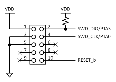
The minimal circuit I posted above has been used OK with a FRDM-KL25 used as programmer board using USBDM.
I suggest you try this arrangement with USBDM as a sanity check i.e. a known working arrangement identical to your hardware.
The KL chips can be hard to reset "fresh" from the factory as they may be in a reset loop. Still, most programmers should be able to cope with this.
As a side note. You appear to be using pins 7 & 9 of the SWD connector for a serial port. I suggest you not use pin 7 as it reserved for a key pin so (in theory) there will be some programming cables that will not be able to be physically connected to your board.
bye
- Mark as New
- Bookmark
- Subscribe
- Mute
- Subscribe to RSS Feed
- Permalink
- Report Inappropriate Content
Hi, pgo,
Thanks for your suggestions.
First, I will try USBDM to find out if it can work on that board.
It is really surprised to me to know that KL chips are hard to reset. Does FSL mention that in some documents? I did spent hours to find how to reset it properly. When it is powered up, the reset is kept on 1.5V (half VCC) with 10K pull-up resistor. I tried to replace pull-up with 1K/470R/220R/100R, I can only get the reset on 2V, but that really bugs me. And it doesn't work at all.
For my understanding, reset should be Schimitt trigger, which is totally works as input with high impedance. A 10K pull-up should be able to pull reset pin to VCC. I have no idea why it only pulls it on 1.5V.
PIN7/PIN9 are designed for RX/TX, but I will drop this since I have already realize that is risky.
- Mark as New
- Bookmark
- Subscribe
- Mute
- Subscribe to RSS Feed
- Permalink
- Report Inappropriate Content
Hi Kai,
A Kinetis chip with an invalid program may suffer from several kinds of program errors:
- Failure to reset or disable the watchdog timer
- Bus lockup on illegal program execution (illegal instruction or illegal address etc)
These will lead to the chip resetting itself.
This can be observed by examining the reset pin with an oscilloscope. It will be seen to be pulsing low by itself.
This can lead to problems since a reset may occur part way through the connection sequence.
bye
- Mark as New
- Bookmark
- Subscribe
- Mute
- Subscribe to RSS Feed
- Permalink
- Report Inappropriate Content
This morning I have tried CoLinkEX to access all four boards at hand. Only one can be connected, programmed and verified in Coocox's CoFlash. I verified the level of reset, it is 3V.
I am still trying to make a device description file for KL25Z used in Keil/Coocox driver to debug the chip.
However, when I connect these four boards to USBDM (Kinetis) in ARM programmer, none can be connected.
Interface tab: USBDM-OPENSDA-A0001 detected
Target tab: Device detect =>
Connection with target has failed.
Please cycle power to the target (measured vcc to gnd, 3V)
Retry connection?
Failed to detect chips
Reason: BDM has no connection to target.
Advanced tab:
Should I try to load OpenSDAMassEraseKinetis.sx to mass erase target KL25Z?
Lab 1
I have used OpenSDAMassEraseKinetis to earse external KL25Z by removing J11/J4 jumpers. And I followed the instructions from OpenSDAMassEraseKinetis.txt. By power up cycle, the LED flash rate keep 50% on/off.
What's going wrong?
Lab 2
I used SEGGER J-Flash ARM, it can be detected via SWD, however I am using a clone version of J-Link. So ... Keil refused to work with a clone version.
Lab 3
Now I am using J-LINK lite for OpenSDA, the device can be connected via SWD in J-Flash. But reading back memory is failed .
RAM check failed @ address 0x1FFFF000.
Write: 0x03020100 07060504
Read: 0x00000000 00000000
(0 bytes of RAM have been checked successfully)
Failed to check blank target.
Maybe SWD_DIO has bad connection ? But if can be connected, DIO should be good.
It seems I should visit FSL.
- Mark as New
- Bookmark
- Subscribe
- Mute
- Subscribe to RSS Feed
- Permalink
- Report Inappropriate Content
- Mark as New
- Bookmark
- Subscribe
- Mute
- Subscribe to RSS Feed
- Permalink
- Report Inappropriate Content
Hi, pgo,
Thanks. I will check the decouping caps.
- Mark as New
- Bookmark
- Subscribe
- Mute
- Subscribe to RSS Feed
- Permalink
- Report Inappropriate Content
Hi pgo,
why you do not put a pull-up resister in swdio pin ?
- Mark as New
- Bookmark
- Subscribe
- Mute
- Subscribe to RSS Feed
- Permalink
- Report Inappropriate Content
The most basic circuitry you need is the power rail [VDD and VSS] connections, the decoupling capacitors for VDD, and pull-up resistors in the RST and SWD_DIO pins. By default the MCU starts up in FEI mode, thus; there is no need to use an external CLK source such as a XTAL. Also be very mindful of the cable connecting between your programming probe and the mcu; it must not be longer than 4 inches.
- Mark as New
- Bookmark
- Subscribe
- Mute
- Subscribe to RSS Feed
- Permalink
- Report Inappropriate Content
Thanks Pedro,
I don't have pull up resistors on SWD_DIO as well as RESET. For my understanding, The pull-up is useful in JTAG debugger JTAG_TMS. The pull up resistor maybe drawn somewhere in reset circuit.
Anyway, I will try to check them all over again.
