- Forums
- Product Forums
- General Purpose MicrocontrollersGeneral Purpose Microcontrollers
- i.MX Forumsi.MX Forums
- QorIQ Processing PlatformsQorIQ Processing Platforms
- Identification and SecurityIdentification and Security
- Power ManagementPower Management
- Wireless ConnectivityWireless Connectivity
- RFID / NFCRFID / NFC
- Advanced AnalogAdvanced Analog
- MCX Microcontrollers
- S32G
- S32K
- S32V
- MPC5xxx
- Other NXP Products
- S12 / MagniV Microcontrollers
- Powertrain and Electrification Analog Drivers
- Sensors
- Vybrid Processors
- Digital Signal Controllers
- 8-bit Microcontrollers
- ColdFire/68K Microcontrollers and Processors
- PowerQUICC Processors
- OSBDM and TBDML
- S32M
- S32Z/E
-
- Solution Forums
- Software Forums
- MCUXpresso Software and ToolsMCUXpresso Software and Tools
- CodeWarriorCodeWarrior
- MQX Software SolutionsMQX Software Solutions
- Model-Based Design Toolbox (MBDT)Model-Based Design Toolbox (MBDT)
- FreeMASTER
- eIQ Machine Learning Software
- Embedded Software and Tools Clinic
- S32 SDK
- S32 Design Studio
- GUI Guider
- Zephyr Project
- Voice Technology
- Application Software Packs
- Secure Provisioning SDK (SPSDK)
- Processor Expert Software
- Generative AI & LLMs
-
- Topics
- Mobile Robotics - Drones and RoversMobile Robotics - Drones and Rovers
- NXP Training ContentNXP Training Content
- University ProgramsUniversity Programs
- Rapid IoT
- NXP Designs
- SafeAssure-Community
- OSS Security & Maintenance
- Using Our Community
-
- Cloud Lab Forums
-
- Knowledge Bases
- ARM Microcontrollers
- i.MX Processors
- Identification and Security
- Model-Based Design Toolbox (MBDT)
- QorIQ Processing Platforms
- S32 Automotive Processing Platform
- Wireless Connectivity
- CodeWarrior
- MCUXpresso Suite of Software and Tools
- MQX Software Solutions
- RFID / NFC
- Advanced Analog
-
- NXP Tech Blogs
- Home
- :
- i.MX Forums
- :
- i.MX Processors
- :
- [iMX8MP] DDR4 data bit/byte swapping
[iMX8MP] DDR4 data bit/byte swapping
- Subscribe to RSS Feed
- Mark Topic as New
- Mark Topic as Read
- Float this Topic for Current User
- Bookmark
- Subscribe
- Mute
- Printer Friendly Page
[iMX8MP] DDR4 data bit/byte swapping
- Mark as New
- Bookmark
- Subscribe
- Mute
- Subscribe to RSS Feed
- Permalink
- Report Inappropriate Content
Dear Community,
We are about to design our custom iMX8M Plus based CPU board. We will use the same DDR4 memory (MT40A512M16LY-062E) as in the reference design of iMX8M Mini EVK (8MMINID4-EVK) but with half of capacity (8Gb or 1GB).
In the mentioned reference design, there seems to be bit-swapping of data lines between the DDRAM and the iMX8M Mini :
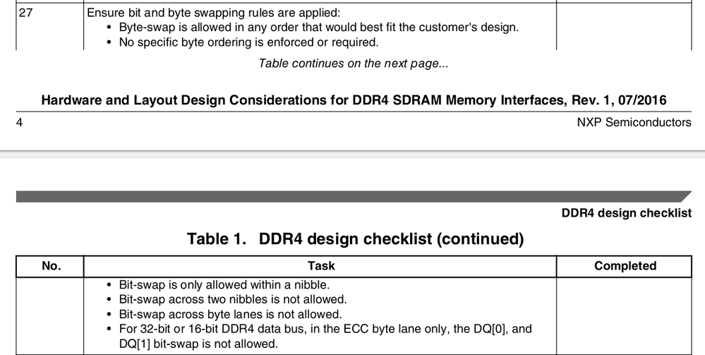
We also need to apply certain bit swapping to optimize the PCB layout and our own bit swapping would be different from above reference design. Therefore, I would like to know where to find the rules of DDR data bit/byte swapping applied for iMX8M Plus, please ? I found following article and application note (AN5097) which seem to be relevant : https://community.nxp.com/t5/Layerscape/AN5097-DDR4-Layout-Checklist-Clarification-for-LS1028A/td-p/...
AN5097 :
I would like to know if above rules should also be applied for the iMX8M Plus ?
Last question, what/where would take into account this bit swapping so that the DDRAM could work correctly : DDR RPA for the timing code generation or else where in u-Boot, please ?
Thanks in advance and best regards,
Khang
- Mark as New
- Bookmark
- Subscribe
- Mute
- Subscribe to RSS Feed
- Permalink
- Report Inappropriate Content
Hi again, CC : @weidong_sun ,
I found the following discussion in which you said :
For DDR4, there is no restriction on the exchange of data bits, as you can see in this design files.
How can I interpret above statement correctly (i.e how can I configure this swapping correctly), please ? Seeing that there's no explicit BoardDataBusConfig tab in the MX8M_Plus_DDR4_RPA_v5.xlsx, but in MX8M_Plus_LPDDR4_RPA_v7.xlsx as below :
Thanks and best regards,
Khang.


