
- NXP Forums
- Product Forums
- General Purpose MicrocontrollersGeneral Purpose Microcontrollers
- i.MX Forumsi.MX Forums
- QorIQ Processing PlatformsQorIQ Processing Platforms
- Identification and SecurityIdentification and Security
- Power ManagementPower Management
- MCX Microcontrollers
- S32G
- S32K
- S32V
- MPC5xxx
- Other NXP Products
- Wireless Connectivity
- S12 / MagniV Microcontrollers
- Powertrain and Electrification Analog Drivers
- Sensors
- Vybrid Processors
- Digital Signal Controllers
- 8-bit Microcontrollers
- ColdFire/68K Microcontrollers and Processors
- PowerQUICC Processors
- OSBDM and TBDML
-
- Solution Forums
- Software Forums
- MCUXpresso Software and ToolsMCUXpresso Software and Tools
- CodeWarriorCodeWarrior
- MQX Software SolutionsMQX Software Solutions
- Model-Based Design Toolbox (MBDT)Model-Based Design Toolbox (MBDT)
- FreeMASTER
- eIQ Machine Learning Software
- Embedded Software and Tools Clinic
- S32 SDK
- S32 Design Studio
- Vigiles
- GUI Guider
- Zephyr Project
- Voice Technology
- Application Software Packs
- Secure Provisioning SDK (SPSDK)
- Processor Expert Software
-
- Topics
- Mobile Robotics - Drones and RoversMobile Robotics - Drones and Rovers
- NXP Training ContentNXP Training Content
- University ProgramsUniversity Programs
- Rapid IoT
- NXP Designs
- SafeAssure-Community
- OSS Security & Maintenance
- Using Our Community
-
-
- Home
- :
- Identification and Security
- :
- NFC
- :
- Re: Problem Reading Mifare cards on PN532 Customized board.
Problem Reading Mifare cards on PN532 Customized board.
- Subscribe to RSS Feed
- Mark Topic as New
- Mark Topic as Read
- Float this Topic for Current User
- Bookmark
- Subscribe
- Mute
- Printer Friendly Page
Problem Reading Mifare cards on PN532 Customized board.
- Mark as New
- Bookmark
- Subscribe
- Mute
- Subscribe to RSS Feed
- Permalink
- Report Inappropriate Content
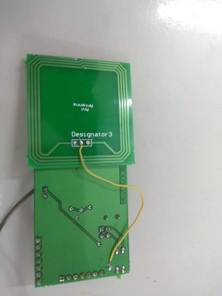
Antenna pn532 NXP
I have customized my own PN532 board.
1. For first assembly the board was working some time and some time it did not.(was getting i2c address , card read some time and other time it did not read the i2c address).without ground tap in antenna
2. Second time same board i assembled i am able to read i2c every time. but it is not able to read any card.
i tried nfc energy harvesting ic so without ground tap on antenna it showed no power, led glowed very less. then i ground tapped antenna so i was able to get full glow on LED on board energy harvesting ic. but still not able to read cards.
attaching the Schematic and board image
- Mark as New
- Bookmark
- Subscribe
- Mute
- Subscribe to RSS Feed
- Permalink
- Report Inappropriate Content
Hello,
Please help us to provide more information on below questions:
1. May I ask what is the purpose of the yellow wire in front of the antenna?

2. Is this connected to a ground plane in the antenna on an inner layer?
3. Why are the inductors different, or is this a typo?

.jpeg)
Best regards,
Ivan.
- Mark as New
- Bookmark
- Subscribe
- Mute
- Subscribe to RSS Feed
- Permalink
- Report Inappropriate Content
Hii Ivan
- Mark as New
- Bookmark
- Subscribe
- Mute
- Subscribe to RSS Feed
- Permalink
- Report Inappropriate Content
Hello,
Please remove the ground from the antenna, only the matching circuit is ok to ground it. Please measure the antenna parameters with a Network analyzer e.g. a MiniVNA and match it correctly to the front-end so that it is correctly tuned at 13,56 MHz. Also please refer to the antenna design guide available in the following link: https://www.nxp.com/docs/en/application-note/AN1445_An1444.zip
Best regards,
Ivan.
- Mark as New
- Bookmark
- Subscribe
- Mute
- Subscribe to RSS Feed
- Permalink
- Report Inappropriate Content
Hii Ivan
1. The yellow wire is used to connect antenna ground tap to board ground
that is VSS.
2. Its a double side PTH board no inner layer.
3. Its a typo value 560nh both.( i have corrected in schematic after
attaching the files)
Also i wanted to ask they are TVSS1 AND TVSS2 transmitter ground on chip
different from other ground(VSS). should i use them for antenna ground
tapping while not shorting it to VSS (keeping them separate)
Thanks
Anmol Kohli
BTech-2016 Electronics Engineer
Embedded Design Engineer
m:+91-9958811944 e: anmol.workmails@gmail.com