- Forums
- Product Forums
- General Purpose MicrocontrollersGeneral Purpose Microcontrollers
- i.MX Forumsi.MX Forums
- QorIQ Processing PlatformsQorIQ Processing Platforms
- Identification and SecurityIdentification and Security
- Power ManagementPower Management
- Wireless ConnectivityWireless Connectivity
- RFID / NFCRFID / NFC
- MCX Microcontrollers
- S32G
- S32K
- S32V
- MPC5xxx
- Other NXP Products
- S12 / MagniV Microcontrollers
- Powertrain and Electrification Analog Drivers
- Sensors
- Vybrid Processors
- Digital Signal Controllers
- 8-bit Microcontrollers
- ColdFire/68K Microcontrollers and Processors
- PowerQUICC Processors
- OSBDM and TBDML
- S32M
-
- Solution Forums
- Software Forums
- MCUXpresso Software and ToolsMCUXpresso Software and Tools
- CodeWarriorCodeWarrior
- MQX Software SolutionsMQX Software Solutions
- Model-Based Design Toolbox (MBDT)Model-Based Design Toolbox (MBDT)
- FreeMASTER
- eIQ Machine Learning Software
- Embedded Software and Tools Clinic
- S32 SDK
- S32 Design Studio
- GUI Guider
- Zephyr Project
- Voice Technology
- Application Software Packs
- Secure Provisioning SDK (SPSDK)
- Processor Expert Software
-
- Topics
- Mobile Robotics - Drones and RoversMobile Robotics - Drones and Rovers
- NXP Training ContentNXP Training Content
- University ProgramsUniversity Programs
- Rapid IoT
- NXP Designs
- SafeAssure-Community
- OSS Security & Maintenance
- Using Our Community
-
- Cloud Lab Forums
-
- Knowledge Bases
- ARM Microcontrollers
- i.MX Processors
- Identification and Security
- Model-Based Design Toolbox (MBDT)
- QorIQ Processing Platforms
- S32 Automotive Processing Platform
- Wireless Connectivity
- CodeWarrior
- MCUXpresso Suite of Software and Tools
- MQX Software Solutions
- RFID / NFC
-
Flash Usage - Block Type
10-16-2018
01:04 PM
1,372 次查看
wayneyounghoney
Contributor I
I have some questions on the Flash system:
- Is there any significance or meaning to the Block Type attribute (Low/Mid/High/Large)? Is it some convention indicating where they are located in the memory map, although "High" doesn't seem to be in the high area and "Large" doesn't seem to fit the other terms.
- Can someone confirm that you can execute code from the lower flash areas (RWW 0,1,2,3,4,5):
Start address End address Allocated size (KB) RWW partition Block number Block type Example use 0x00000000 0x0000FFFF 64 0 0 Low EEPROM data 0x00010000 0x0001FFFF 64 1 1 Low EEPROM data 0x00020000 0x0002FFFF 64 2 0 Mid EEPROM data 0x00030000 0x0003FFFF 64 3 1 Mid EEPROM data 0x00040000 0x003FFFFF 3840 — — Not available n/a 0x00400000 0x00403FFF 16 0 0 UTEST See Table 4-3 0x00404000 0x005FFFFF 2032 — — Not available n/a 0x00600000 0x00603FFF 16 4 0 High CSE 0x00604000 0x00607FFF 16 5 1 High CSE
- Why do RWWs 0,2 have a Block 0 but RWWs 1, 3 have a Block 1 (and not a Block 0)? Any significance to this?
- If you do not use the CSE can the RWW 4 and 5 be used for any code or data use?
- The total available Flash is 8480KB (8192KB of Large and 288KB of Low/Mid/High)
5 回复数
10-18-2018
06:00 AM
1,212 次查看
NXP TechSupport
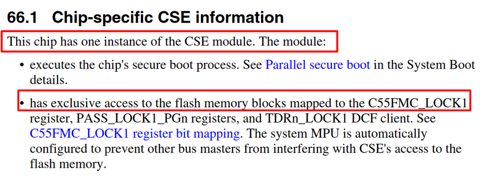
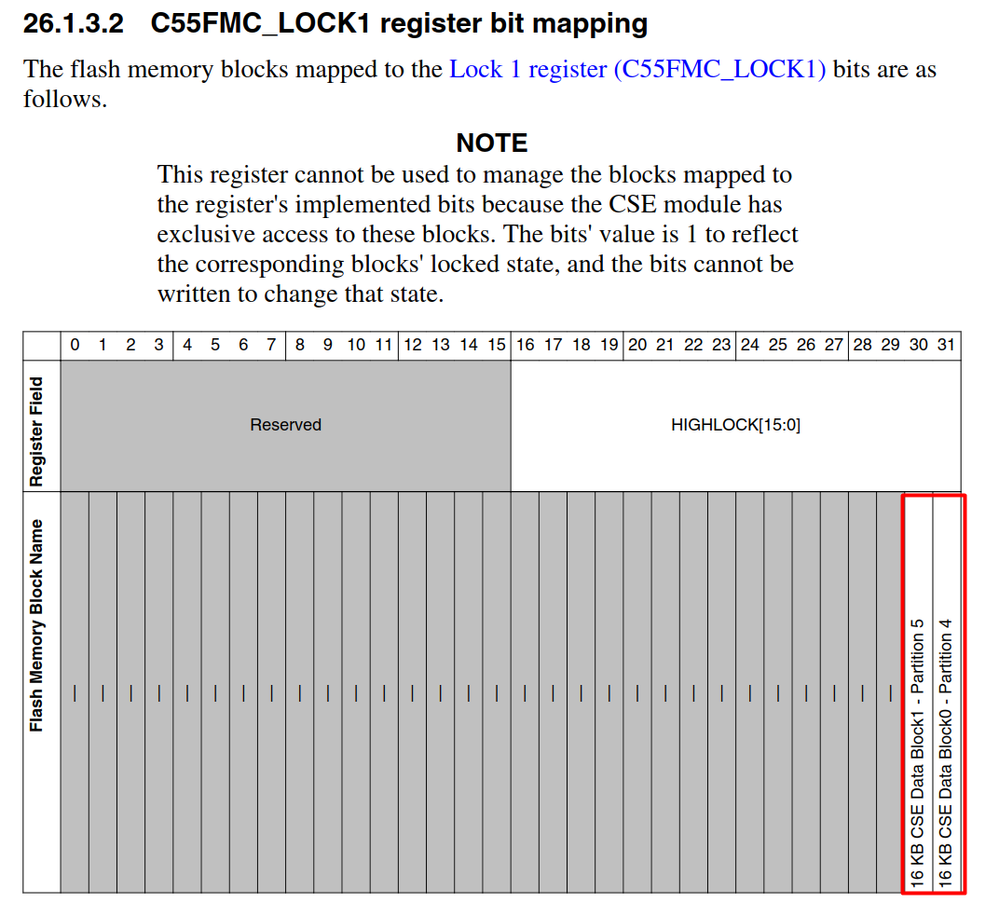
CSE flash blocks cannot be used for general purpose functionality because of reason below:
11-07-2018
07:48 AM
1,212 次查看
wayneyounghoney
Contributor I
Hi David. Thanks for the info. I appreciate it.
10-17-2018
08:34 AM
1,212 次查看
NXP TechSupport
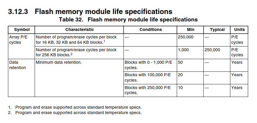
The block type affects mainly endurance and data retention as you can see below (datasheet screenshot):
You can execute code from the lower flash areas, but areas with higher endurance (smaller block) are mainly intended for EEPROM emulation, but you can execute code from these area as well. I am not completely sure about CSE blocks, I am finding it out, returning to you.
Regarding blocks and partitions, blocks are numbered in ascending order withing one block type, partitions the same way withing the whole flash. Just matter of implementation.


