
- Forums
- Product Forums
- General Purpose MicrocontrollersGeneral Purpose Microcontrollers
- i.MX Forumsi.MX Forums
- QorIQ Processing PlatformsQorIQ Processing Platforms
- Identification and SecurityIdentification and Security
- Power ManagementPower Management
- Wireless ConnectivityWireless Connectivity
- RFID / NFCRFID / NFC
- Advanced AnalogAdvanced Analog
- Neural Processing UnitsNeural Processing Units
- MCX Microcontrollers
- S32G
- S32K
- S32V
- MPC5xxx
- Other NXP Products
- S12 / MagniV Microcontrollers
- Powertrain and Electrification Analog Drivers
- Sensors
- Vybrid Processors
- Digital Signal Controllers
- 8-bit Microcontrollers
- ColdFire/68K Microcontrollers and Processors
- PowerQUICC Processors
- OSBDM and TBDML
- S32M
- S32Z/E
-
- Solution Forums
- Software Forums
- MCUXpresso Software and ToolsMCUXpresso Software and Tools
- CodeWarriorCodeWarrior
- MQX Software SolutionsMQX Software Solutions
- Model-Based Design Toolbox (MBDT)Model-Based Design Toolbox (MBDT)
- FreeMASTER
- eIQ Machine Learning Software
- Embedded Software and Tools Clinic
- S32 SDK
- S32 Design Studio
- GUI Guider
- Zephyr Project
- Voice Technology
- Application Software Packs
- Secure Provisioning SDK (SPSDK)
- Processor Expert Software
- Generative AI & LLMs
-
- Topics
- Mobile Robotics - Drones and RoversMobile Robotics - Drones and Rovers
- NXP Training ContentNXP Training Content
- University ProgramsUniversity Programs
- Rapid IoT
- NXP Designs
- SafeAssure-Community
- OSS Security & Maintenance
- Using Our Community
-
- Cloud Lab Forums
-
- Knowledge Bases
- ARM Microcontrollers
- i.MX Processors
- Identification and Security
- Model-Based Design Toolbox (MBDT)
- QorIQ Processing Platforms
- S32 Automotive Processing Platform
- Wireless Connectivity
- CodeWarrior
- MCUXpresso Suite of Software and Tools
- MQX Software Solutions
- RFID / NFC
- Advanced Analog
- Neural Processing Units
-
- NXP Tech Blogs
Hi NXP Community,
I am attempting to connect an LPC Link2 board to a beagle bone black (BBB) via I2C with the Link2 as the slave device. I believe for this to work I need to receive a clock signal from the BBB and input it into the Link2 via pin k6 on the LPC4370.
On the Link2 schematic sheet (provided below), k6 is accessible via TP_CLK2. The issue is that on the Link2 itself, the test points are not labelled (aside from the 3V3 and GND TPs).
Can someone provide some information on what all the test points are connected to on the Link2?
Regards,
Quinn
已解决! 转到解答。
> Yes so don't I need to input the clock signal from the Beaglebone Black into the Link2?
Check out the I2C spec., e.g. at Wikipedia.
I2C uses 3 connections, SDA (serial data), SCL (serial clock) and GND. This clock (SCL) is a I2C bus signal, and not directly related to the core clock (but derived from it).
Be aware that both signal are bidirectional, more or less. The SDA direction is switched for the ACK bit in every transmission, and SCL can be held down by the slave for "clock stretching" (if supported). My point, trying other non-I2C signal pins might damage the hardware.
> If so I need to do it via a test point on the Link2 but none of them are labeled.
Those test points are for production tests only, not for application use. This is why they are not labelled. They might be labelled at the PCB layout plan, which is part of the schematics.
> I believe both have logic levels of 3.3V.
I would better make sure. A 3.3V level can definitely damage 1.8V electronics, at best you just don't get it to work.
> I believe for this to work I need to receive a clock signal from the BBB and input it into the Link2 via pin k6 on the LPC4370.
I am not sure what you mean.
The I2C bus has a SCL signal as clock, which is provided by the (bus) master. Which is the BB in this case.
PS:
Have you checked both bords/signals have the same signal level ? Didn't the BB have 1.8V ? In this case, you need level shifters.
>The I2C bus has a SCL signal as clock, which is provided by the (bus) master. Which is the BB in this case.
Yes so don't I need to input the clock signal from the Beaglebone Black into the Link2? If so I need to do it via a test point on the Link2 but none of them are labeled.
>Have you checked both bords/signals have the same signal level ? Didn't the BB have 1.8V ? In this case, you need level shifters.
I believe both have logic levels of 3.3V.
> Yes so don't I need to input the clock signal from the Beaglebone Black into the Link2?
Check out the I2C spec., e.g. at Wikipedia.
I2C uses 3 connections, SDA (serial data), SCL (serial clock) and GND. This clock (SCL) is a I2C bus signal, and not directly related to the core clock (but derived from it).
Be aware that both signal are bidirectional, more or less. The SDA direction is switched for the ACK bit in every transmission, and SCL can be held down by the slave for "clock stretching" (if supported). My point, trying other non-I2C signal pins might damage the hardware.
> If so I need to do it via a test point on the Link2 but none of them are labeled.
Those test points are for production tests only, not for application use. This is why they are not labelled. They might be labelled at the PCB layout plan, which is part of the schematics.
> I believe both have logic levels of 3.3V.
I would better make sure. A 3.3V level can definitely damage 1.8V electronics, at best you just don't get it to work.
Ok I was confused by the image attached of the transmitter slave mode. I thought that I needed to input data/clock sources into TX_SDA/SCK pins but the RX_SDA/SCK pins are both TX_and RX_.
This is my first time using I2C so still working it all out.
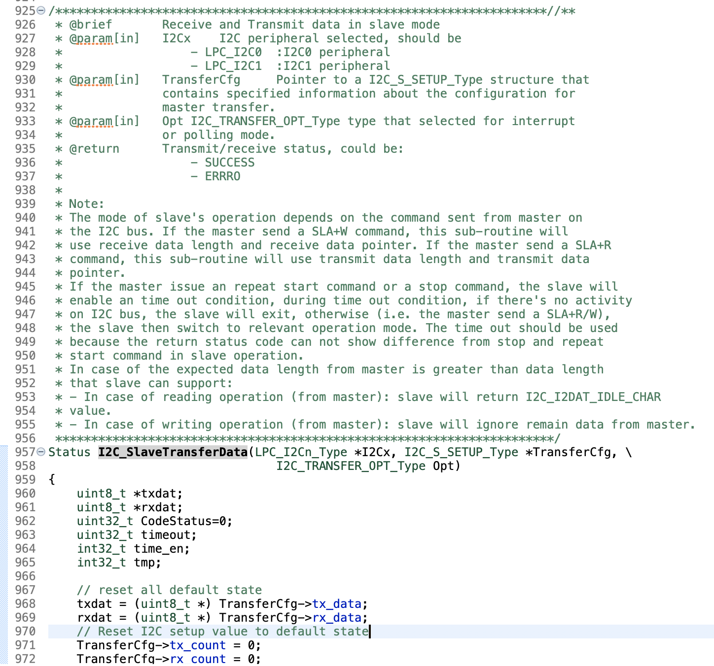
Next I need to figure out how to use the function in the code image (in lpc43xx_i2c.c). Hopefully it configures the pins in the way I am expecting. I might post more questions about it here. Thanks for your help so far.
Quinn