- Forums
- Product Forums
- General Purpose MicrocontrollersGeneral Purpose Microcontrollers
- i.MX Forumsi.MX Forums
- QorIQ Processing PlatformsQorIQ Processing Platforms
- Identification and SecurityIdentification and Security
- Power ManagementPower Management
- Wireless ConnectivityWireless Connectivity
- RFID / NFCRFID / NFC
- Advanced AnalogAdvanced Analog
- MCX Microcontrollers
- S32G
- S32K
- S32V
- MPC5xxx
- Other NXP Products
- S12 / MagniV Microcontrollers
- Powertrain and Electrification Analog Drivers
- Sensors
- Vybrid Processors
- Digital Signal Controllers
- 8-bit Microcontrollers
- ColdFire/68K Microcontrollers and Processors
- PowerQUICC Processors
- OSBDM and TBDML
- S32M
- S32Z/E
-
- Solution Forums
- Software Forums
- MCUXpresso Software and ToolsMCUXpresso Software and Tools
- CodeWarriorCodeWarrior
- MQX Software SolutionsMQX Software Solutions
- Model-Based Design Toolbox (MBDT)Model-Based Design Toolbox (MBDT)
- FreeMASTER
- eIQ Machine Learning Software
- Embedded Software and Tools Clinic
- S32 SDK
- S32 Design Studio
- GUI Guider
- Zephyr Project
- Voice Technology
- Application Software Packs
- Secure Provisioning SDK (SPSDK)
- Processor Expert Software
- Generative AI & LLMs
-
- Topics
- Mobile Robotics - Drones and RoversMobile Robotics - Drones and Rovers
- NXP Training ContentNXP Training Content
- University ProgramsUniversity Programs
- Rapid IoT
- NXP Designs
- SafeAssure-Community
- OSS Security & Maintenance
- Using Our Community
-
- Cloud Lab Forums
-
- Knowledge Bases
- ARM Microcontrollers
- i.MX Processors
- Identification and Security
- Model-Based Design Toolbox (MBDT)
- QorIQ Processing Platforms
- S32 Automotive Processing Platform
- Wireless Connectivity
- CodeWarrior
- MCUXpresso Suite of Software and Tools
- MQX Software Solutions
- RFID / NFC
- Advanced Analog
-
- NXP Tech Blogs
- Home
- :
- 汎用マイクロコントローラ
- :
- LPCマイクロコントローラ
- :
- Re: How can i set up to create CLOCK for External (CLKOUT)?
How can i set up to create CLOCK for External (CLKOUT)?
- RSS フィードを購読する
- トピックを新着としてマーク
- トピックを既読としてマーク
- このトピックを現在のユーザーにフロートします
- ブックマーク
- 購読
- ミュート
- 印刷用ページ
- 新着としてマーク
- ブックマーク
- 購読
- ミュート
- RSS フィードを購読する
- ハイライト
- 印刷
- 不適切なコンテンツを報告
Dear friend,
Working Environment.
Testing Board : LPC-LINK2
MCU : LPC4370
Develop Tools : LPCXpresso (free) and LPCOpen (demo code)
Main Test Interface : ADCHS
Main Test Peripheral : LINE SCANNER by ADCHS
I am working to testing ADCHS on LPC-link2 board that is using LPC4370 MCU.
My result is the following after analysis of MY project.
- I have to get ADCHS value from LINE SCANNER that is working 8MHz clock. So I have to create external clock for LINE_SCANNER
- This Clock will be connected to ADCHS external triggers for triggering.
- I saw Manual (UM10503-USER-Manual) section 48.7.6 and Section 18.4.25
Please let me your solution to create clock for LPC4370 in LPC-link2 board.
- Am I right analysis for connecting and getting ADCHS with LINE SCANNER ?
- I am doing to create Clock which is 8MHz to out CLKOUT (P1_19 port)
- How can I set up to make 8MHz clock that will be route P1_19 for CLKOUT ?
解決済! 解決策の投稿を見る。
- 新着としてマーク
- ブックマーク
- 購読
- ミュート
- RSS フィードを購読する
- ハイライト
- 印刷
- 不適切なコンテンツを報告
Hi LEE Young Jae,
Thanks for your reply. I think I missed one information before.
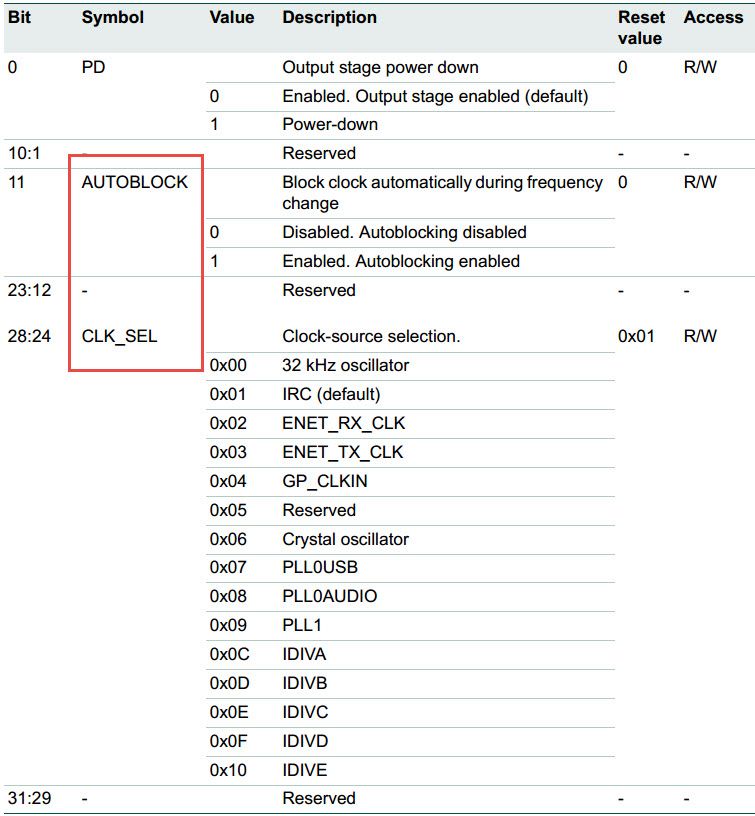
To generate the clock via the CLKOUT pin ( you choose the P1_19), you need to active clock block and select clock source simultaneously via the BSE_OUT_CLK register at first. Next to configure the P1_19 to output clock via the Pin configuration register as the Table 192 illustrates.
In the previous reply, I pointed out that hardware triggers is not necessary to connect some additional PWM to trigger the ADCHS,
The internal hardware trigger will connect the ADCHS automatically via configuring the GIMA module.
Hope this is clear.
Have a great day,
TIC
-----------------------------------------------------------------------------------------------------------------------
Note: If this post answers your question, please click the Correct Answer button. Thank you!
-----------------------------------------------------------------------------------------------------------------------
- 新着としてマーク
- ブックマーク
- 購読
- ミュート
- RSS フィードを購読する
- ハイライト
- 印刷
- 不適切なコンテンツを報告
Hi LEE Young Jae,
Thank you for your interest in NXP Semiconductor products and the opportunity to serve you.
1) Am I right analysis for connecting and getting ADCHS with LINE SCANNER ?
No, you're incorrect. The hardware triggers is not necessary to connect some additional PWM to trigger the ADCHS.
Have a great day,
TIC
-----------------------------------------------------------------------------------------------------------------------
Note: If this post answers your question, please click the Correct Answer button. Thank you!
-----------------------------------------------------------------------------------------------------------------------
- 新着としてマーク
- ブックマーク
- 購読
- ミュート
- RSS フィードを購読する
- ハイライト
- 印刷
- 不適切なコンテンツを報告
HI jeremyzhou,
How can i set up (configure) ADCHS device with additional device (Line Scanner).
Additional device is Line Scanner that is need external clock(8MHz) for output analog result.
if you have idea for LPC4370 environment, Please let me know step by step .
Thanks.
- 新着としてマーク
- ブックマーク
- 購読
- ミュート
- RSS フィードを購読する
- ハイライト
- 印刷
- 不適切なコンテンツを報告
Hi LEE Young Jae,
Thanks for your reply. I think I missed one information before.
To generate the clock via the CLKOUT pin ( you choose the P1_19), you need to active clock block and select clock source simultaneously via the BSE_OUT_CLK register at first. Next to configure the P1_19 to output clock via the Pin configuration register as the Table 192 illustrates.
In the previous reply, I pointed out that hardware triggers is not necessary to connect some additional PWM to trigger the ADCHS,
The internal hardware trigger will connect the ADCHS automatically via configuring the GIMA module.
Hope this is clear.
Have a great day,
TIC
-----------------------------------------------------------------------------------------------------------------------
Note: If this post answers your question, please click the Correct Answer button. Thank you!
-----------------------------------------------------------------------------------------------------------------------
