- Forums
- Product Forums
- General Purpose MicrocontrollersGeneral Purpose Microcontrollers
- i.MX Forumsi.MX Forums
- QorIQ Processing PlatformsQorIQ Processing Platforms
- Identification and SecurityIdentification and Security
- Power ManagementPower Management
- Wireless ConnectivityWireless Connectivity
- RFID / NFCRFID / NFC
- Advanced AnalogAdvanced Analog
- MCX Microcontrollers
- S32G
- S32K
- S32V
- MPC5xxx
- Other NXP Products
- S12 / MagniV Microcontrollers
- Powertrain and Electrification Analog Drivers
- Sensors
- Vybrid Processors
- Digital Signal Controllers
- 8-bit Microcontrollers
- ColdFire/68K Microcontrollers and Processors
- PowerQUICC Processors
- OSBDM and TBDML
- S32M
- S32Z/E
-
- Solution Forums
- Software Forums
- MCUXpresso Software and ToolsMCUXpresso Software and Tools
- CodeWarriorCodeWarrior
- MQX Software SolutionsMQX Software Solutions
- Model-Based Design Toolbox (MBDT)Model-Based Design Toolbox (MBDT)
- FreeMASTER
- eIQ Machine Learning Software
- Embedded Software and Tools Clinic
- S32 SDK
- S32 Design Studio
- GUI Guider
- Zephyr Project
- Voice Technology
- Application Software Packs
- Secure Provisioning SDK (SPSDK)
- Processor Expert Software
- Generative AI & LLMs
-
- Topics
- Mobile Robotics - Drones and RoversMobile Robotics - Drones and Rovers
- NXP Training ContentNXP Training Content
- University ProgramsUniversity Programs
- Rapid IoT
- NXP Designs
- SafeAssure-Community
- OSS Security & Maintenance
- Using Our Community
-
- Cloud Lab Forums
-
- Knowledge Bases
- ARM Microcontrollers
- i.MX Processors
- Identification and Security
- Model-Based Design Toolbox (MBDT)
- QorIQ Processing Platforms
- S32 Automotive Processing Platform
- Wireless Connectivity
- CodeWarrior
- MCUXpresso Suite of Software and Tools
- MQX Software Solutions
- RFID / NFC
- Advanced Analog
-
- NXP Tech Blogs
- Home
- :
- 汎用マイクロコントローラ
- :
- Kinetisマイクロコントローラ
- :
- PE multilink JTAG/BDM Kinetis programming issue
PE multilink JTAG/BDM Kinetis programming issue
- RSS フィードを購読する
- トピックを新着としてマーク
- トピックを既読としてマーク
- このトピックを現在のユーザーにフロートします
- ブックマーク
- 購読
- ミュート
- 印刷用ページ
- 新着としてマーク
- ブックマーク
- 購読
- ミュート
- RSS フィードを購読する
- ハイライト
- 印刷
- 不適切なコンテンツを報告
Hi
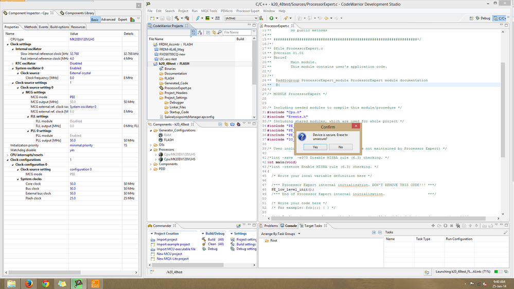
I am trying to program K20 custom board but it is showing an error.
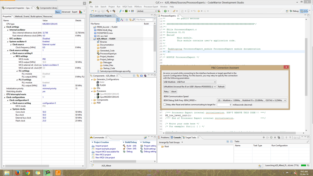
after clicking yes, the same msg appear and again I click yes then following error comes
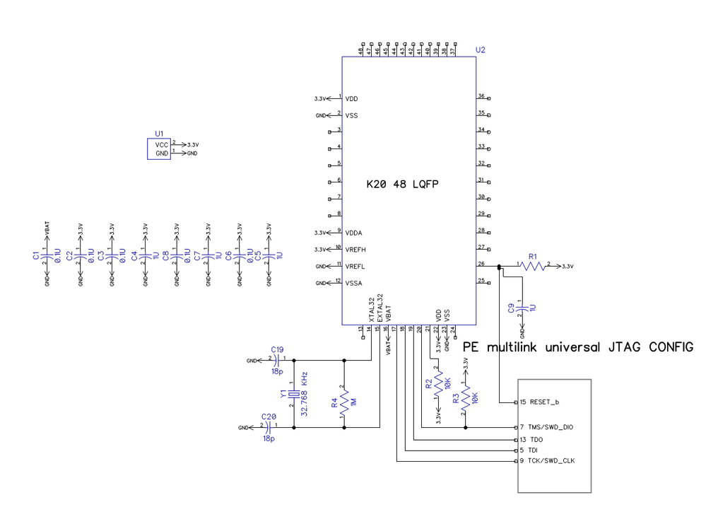
these two error msg comes after one another and it doesn't program. Kindly look into the matter initially I had the same issue for K10 board. I tried everything but It didn't worked. PE multilink universal not detecting K10 uc I thought that there might be some soldering issue as it was a QFN package. so I changed my design and added MK20DX128VLF5(LQFP) we bought 100 pcs of this uc and 100 pc of KL05 , 30 pc of K10. we checked for K10 and K20 uc it doesn't work. I checked PE multilink by programming FRDM-KL46Z board through SWD connecter J6, it is programming the board without any issue. I went through the KQRUG user guide which I found out from my previous query regarding K10 board through the community. and I also went through the PE4576-Technical summary. and tried resolving the issue but didn't resolve then after bashing my head I somehow managed to find an app note on programming kinetis uc i.e AN4835 which I think is supposed to be mention in the datasheet as no user will get to know that there exist an app note for how to program the Kinetis uc. There are many engineers who will be working on ARM cortex uc but if there is not much resources then why will they choose freescale. Kindly look into the matter and make the programmer work as I fear all the above controller i.e (100 K20, 100 Kl05, 30 K10) uc will be collecting dust. Already we have 100 k20 boards ready. The following diagram shows the connections I have tried for different modes(JTAG/SWD) for programming K20 board.
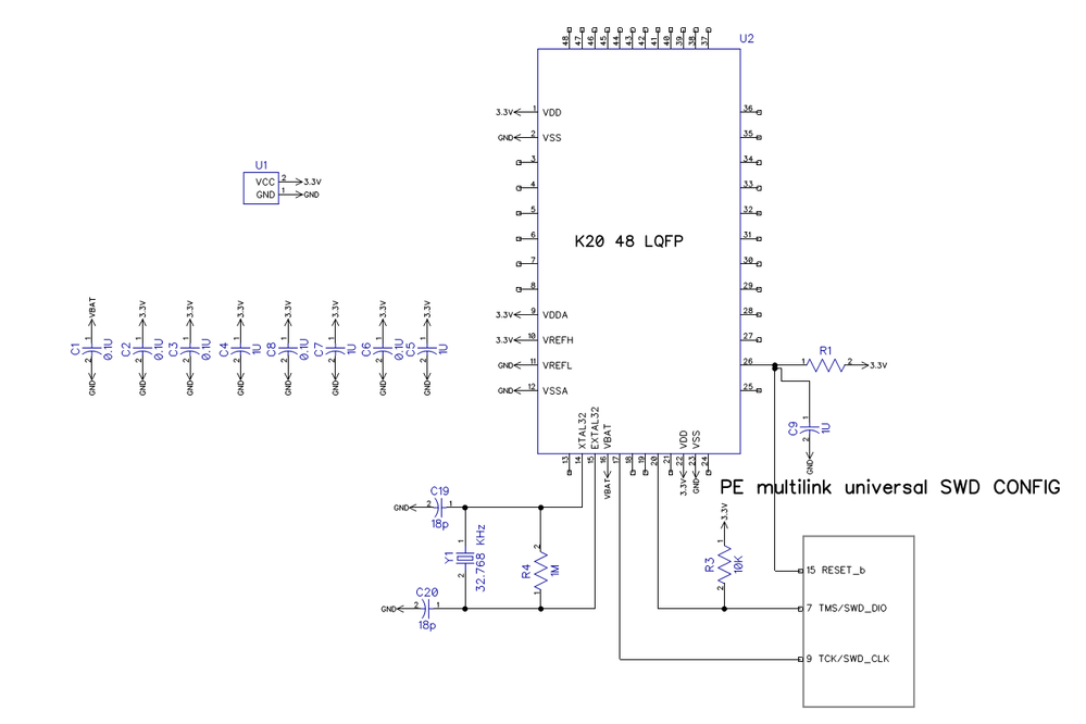
it didn't worked then i tried SWD config
In both the cases I connected VCC(3.3V) ----->TVCC(PIN 1)
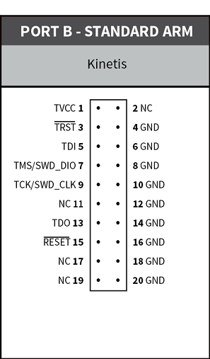
and GND----> GND(PIN 4) of PE multilink universal. I am using the following port from PE multilink universal.
I probed RESET_b pin in normal condition it is logic high(3.3V) and while programming it becomes logic low(0V).
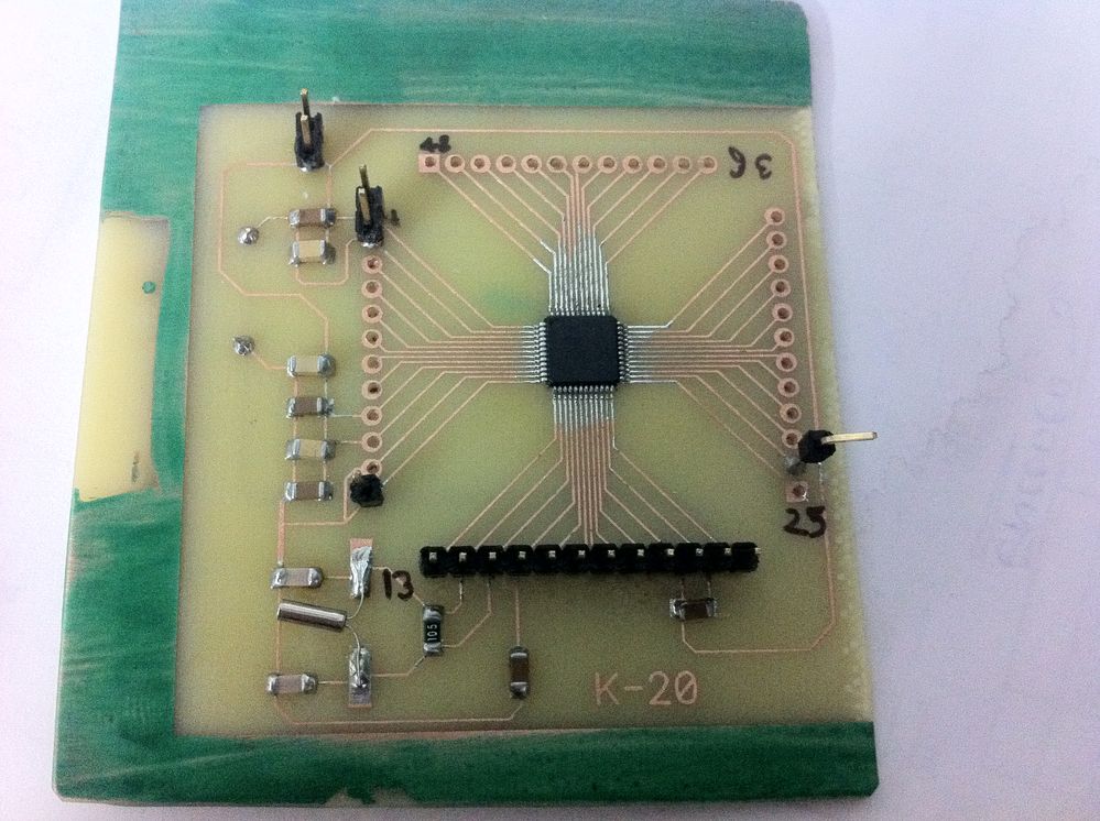
The above is the testing breakout board(dual side).
I hope The community will help me to resolve this issue ASAP. Our expected target is 100,000 kinetis units this year In our line of products.
Thanks and Regards
Amit Kumar
解決済! 解決策の投稿を見る。
- 新着としてマーク
- ブックマーク
- 購読
- ミュート
- RSS フィードを購読する
- ハイライト
- 印刷
- 不適切なコンテンツを報告
Hello Amit:
Thanks for considering my suggestions. About your comments and some more inputs:
5) This should not be critical, but try replacing that 1K resistor with one of 4.7K - 10K. Also confirm that you have the R2 10K pull - up resistor connected to pin 21, and measure voltage in that pin to verify that it is always in high level.
Now, the 1.64 V is definitely not correct, the value should be near the 3.3 V when not asserted. This seems to indicate that the MCU is constantly resetting. You need to watch that pin with an oscilloscope.
If the device is resetting, this may solve the issue:
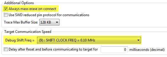
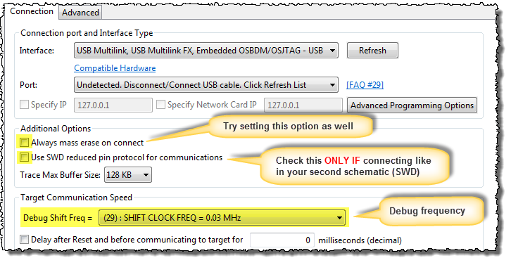
- Make sure to select "Always mass erase on connect", and select a not so high debug frequency (e.g. 0.10 MHz).
Then follow the next steps:
1) Disconnect the board from your 3.3 V source.
2) With a jumper force the reset pin to a low level (GND) and hold it.
3) Power on the board (connect the 3.3 V source). Do not release reset yet.
4) Start a debug session and as soon as it is starting release the reset button.
Try this more than once.
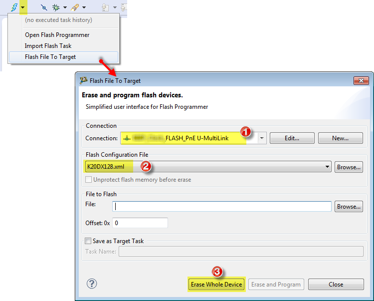
Additionally, you could also try mass erasing the K20 device from the Flash programmer. Just open the programmer, select proper connection and specific flash configuration file and then click on "Erase Whole Device".
If the Erase is successful, then you should be able to debug.
Let me know what you find.
Regards!
Jorge Gonzalez
- 新着としてマーク
- ブックマーク
- 購読
- ミュート
- RSS フィードを購読する
- ハイライト
- 印刷
- 不適切なコンテンツを報告
hello all,
iam trying to program mk60fx512 using multilink fx jtag. Iam getting the following error ...
Device selected is k60fx512
User Specified Hardware Selection : Interface=USBMULTILINK and Port=USB1
Connecting to target.
P&E Interface detected - Flash Version 9.33
Forcing mass erase...
Can not enter background mode .
Unable to initialize PEDebug.
PE-ERROR: Failed to Initialize Target
How to solve this.Please help
- 新着としてマーク
- ブックマーク
- 購読
- ミュート
- RSS フィードを購読する
- ハイライト
- 印刷
- 不適切なコンテンツを報告
Hello Amit, Jorge!!
I want to say thank you about this post, very helpul and give me a lot of advices on how to implement correctly my own k20 custom board. I'am using mk20dx256vlh7, same as Teensy 3.1 onboard.
I have to recognize that it doesn't work at first attempt, but finally done!!
About the problem with SWD debugging, I'm able to use JTAG/SWD, this is thanks to Jose Ribeiro contribution:
"I added a SWD_DIO 10k pullup and a SWD_CLK 4k7 pulldown + 66pF"
Excellent work to all!!
BR
Mario
- 新着としてマーク
- ブックマーク
- 購読
- ミュート
- RSS フィードを購読する
- ハイライト
- 印刷
- 不適切なコンテンツを報告
Hi darla & Amit Kumar
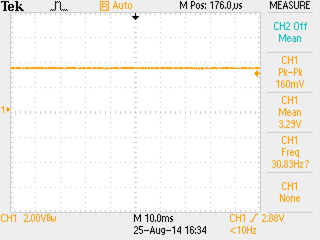
Thank you for your instant replies. EZP_CS_b pin has been pulled high. I have attached reset waveform captured before and after disconnection. What do they imply?
Regards
Kayathri
- 新着としてマーク
- ブックマーク
- 購読
- ミュート
- RSS フィードを購読する
- ハイライト
- 印刷
- 不適切なコンテンツを報告
Hi Kayathri
Can you share the schematic of the reset circuitry? If you are using a cap connected to reset pin please remove it. For flashing the uc u need to remove the cap. but let the 10K pullup be connected to the reset pin. after doing that repeat the steps.
Generally reset pin should show 3.20 V but in your 1st waveform the voltage shown is 2.0 V. Attached is the waveform of reset pin which I have recorded from my K60 board.
Kind Regards
Amit Kumar
- 新着としてマーク
- ブックマーク
- 購読
- ミュート
- RSS フィードを購読する
- ハイライト
- 印刷
- 不適切なコンテンツを報告
Hi,
We are using our customized K70 board. We use JTAG for debugging. Previously it was not debugging at all. After we pulled up the reset pin using 10k, we are able to debug ,but the device gets disconnected after around 2 minutes. Reset pin is also pulsing continuously. Kindly suggest us the steps to be followed further.
Regards,
Kayathri M
- 新着としてマーク
- ブックマーク
- 購読
- ミュート
- RSS フィードを購読する
- ハイライト
- 印刷
- 不適切なコンテンツを報告
Hi Kayathi
Please follow these steps
1. Probe the reset pin and check if the waveform matches with the waveform on this thread. It might be that your uc is still not flashed. In that case follow the instruction How To Sucessfully Program a Custom made Kinetis Microcontroller Board.
2. In case the reset pulsing is random, There might be some soldering issue. or some pins might have been shorted. What is the voltage on reset pin?
Regards
Amit Kumar
- 新着としてマーク
- ブックマーク
- 購読
- ミュート
- RSS フィードを購読する
- ハイライト
- 印刷
- 不適切なコンテンツを報告
Hi kayathi
This is most probably connections issue make sure your connector properly connected and check by direct soldering for verification.
Make sure that EZP_CS_b pin pulled high for JTAG/SWD program.
thanks
darla
- 新着としてマーク
- ブックマーク
- 購読
- ミュート
- RSS フィードを購読する
- ハイライト
- 印刷
- 不適切なコンテンツを報告
Hello Amit:
Let me throw some suggestions and questions trying to help:
1) Are you connecting VSS to GND (MCU pin 23)?. Sorry if this is a silly question, but from your board picture I cannot see the other side and I just see a capacitor in there.
2) Again, most probably you have checked it, but just to make sure, do you see both LEDs ON when connecting your Multilink?
3) You connected GND to PIN 4 of Multilink. The ARM JTAG interface specs recommend to connect all the GND pins, not only pin 4 (pins 4/6/8/10/12/14/16/18/20). This is to reduce noise.\
4) You are not using a standard 20 pin header in your custom board, so I assume you are connecting your Multilink with jumper wires. In this case you have to make sure that these wires are as short as possible. In several cases large cables have caused connection problems.
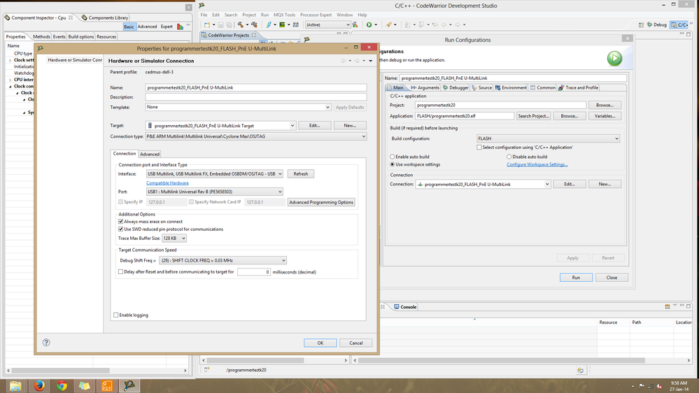
5) Try reducing the PE Universal Multilink debug speed. This can be done from the tab Run -> Debug Configurations -> Edit. As your MCUs are brand new, I also recommend to check the "Always mass erase on connect" option. And last, for your second schematic (using SWD instead of JTAG), you have to make sure to select the "Use SWD ..." option. See the next images for these comments:
6) And finally, I have known of cases in which the debug configurations get corrupted. Easiest way to discard this is to create a new empty bareboard project and trying to program this in your MCU, but considering my points above as well.
I hope some of this guides you to the solution. Let us know about further findings.
Regards!
Jorge Gonzalez
- 新着としてマーク
- ブックマーク
- 購読
- ミュート
- RSS フィードを購読する
- ハイライト
- 印刷
- 不適切なコンテンツを報告
Hi Jorge
Thanks for the quick reply. I have followed your suggestions. what I did was :
1. I removed all the external connections and checked the continuity of the board. vdd(+3.3V) is connected to pin nos 1, 9, 10, 16, 22 and the VSS(GND) is connected to pin nos. 2, 11, 12, 23.(Its a dual sided board)
2. As per the multilink universal guideline i.e its given below, I followed and ensured both the LEDs are glowing.
3. I have connected all the ground pins (2,4,6,8,10,12,14,16,18,20) of multilink externally. (although multimeter shows that all the gnd pins are shorted internally when not connected)
4. I have checked that there is no loose contact with the jumpers, and the length of the jumper is around 15 cm.
5. According to the 1st schematic, value for R1(resistor to reset pin) is 1K. when I probe this pin, In normal condition I get 1.64V and when the programming starts it becomes (0V). Is that expected?? I mean the voltage 1.64v? or should it be higher?
6. I tried your 5th point i.e 1st checked for SWD, and then for JTAG.
7. I tried making empty bareboard project and programming it.
In this case It didn't asked for secure, it directly stated that multilink is not communicating i.e 2nd image which I shared in my 1st post.
The above configuration is for SWD now Trying for JTAG. It still didn't worked. what should I do next?
Thanks and Regards
Amit Kumar
- 新着としてマーク
- ブックマーク
- 購読
- ミュート
- RSS フィードを購読する
- ハイライト
- 印刷
- 不適切なコンテンツを報告
Hello Amit:
Thanks for considering my suggestions. About your comments and some more inputs:
5) This should not be critical, but try replacing that 1K resistor with one of 4.7K - 10K. Also confirm that you have the R2 10K pull - up resistor connected to pin 21, and measure voltage in that pin to verify that it is always in high level.
Now, the 1.64 V is definitely not correct, the value should be near the 3.3 V when not asserted. This seems to indicate that the MCU is constantly resetting. You need to watch that pin with an oscilloscope.
If the device is resetting, this may solve the issue:
- Make sure to select "Always mass erase on connect", and select a not so high debug frequency (e.g. 0.10 MHz).
Then follow the next steps:
1) Disconnect the board from your 3.3 V source.
2) With a jumper force the reset pin to a low level (GND) and hold it.
3) Power on the board (connect the 3.3 V source). Do not release reset yet.
4) Start a debug session and as soon as it is starting release the reset button.
Try this more than once.
Additionally, you could also try mass erasing the K20 device from the Flash programmer. Just open the programmer, select proper connection and specific flash configuration file and then click on "Erase Whole Device".
If the Erase is successful, then you should be able to debug.
Let me know what you find.
Regards!
Jorge Gonzalez
- 新着としてマーク
- ブックマーク
- 購読
- ミュート
- RSS フィードを購読する
- ハイライト
- 印刷
- 不適切なコンテンツを報告
I tried to use Multilink today to program the K22 and ran into this problem. Checking the Multilink, I found R19 and R23 (all 47E) burnt. I changed it and everything works. I checked my board with other Multilink and the board worked, then I checked the Multilink for eventually issue.
- 新着としてマーク
- ブックマーク
- 購読
- ミュート
- RSS フィードを購読する
- ハイライト
- 印刷
- 不適切なコンテンツを報告
Thanks Jorge!!
I made a new board with a different K20 uc and there I added 20 pin header and that got mass erased and is working fine. I was able to program custom made K-60 board also !!!. I think with the controller in which only SWD pins are there for programing, needs to be programmed using SWD mode only and for the controller in which SWD/JTAG and EZport is present needs to be programmed with JTAG mode. I Tried with SWD but that didn't worked JTAG worked successfully there, for KL05 swd worked.
I have also made a post in which I have described the shortcut process.https://community.nxp.com/docs/DOC-99609
but I feel in datasheet it should be mentioned that all new controller should be programmed in a different way for the1st time programming.
Regards
Amit Kumar
- 新着としてマーク
- ブックマーク
- 購読
- ミュート
- RSS フィードを購読する
- ハイライト
- 印刷
- 不適切なコンテンツを報告
Hello Amit:
Sorry I've been a little busy. It is great you finally got positive results!!. I agree about the JTAG/SWD modes (although I am not sure why it did not work in SWD, I will try to investigate this), and also with the mass erase info.
I need to thank you a lot because this thread and the document you just created are going to help many people, as Jon above for example.
Kind Regards!
Jorge Gonzalez
- 新着としてマーク
- ブックマーク
- 購読
- ミュート
- RSS フィードを購読する
- ハイライト
- 印刷
- 不適切なコンテンツを報告
Hello,
I'm now testing our first Kinetis MK22FX512VLK12 custom controller board.
In our design we included a SWD programming connector (VCC, GND, SWD_DIO, SWD_CLK, RESET). These pins are connected to the PEMicro Multilink Universal (firmware v6.10) Port B (TVCC, GND, TMS/SWD_DIO, TCK/SWD_CLK).
After several attempts using the SWD interface I always get a "Device is secure" message on CW 10.6 and KDS 1.1.0. This is the same behavior as described by Amit.
I also managed to tweak the board and I added TDI and TDO. It works, but I'm looking for a way to use SWD interface.
The Kinetis MCUs use JTAG at reset state, but they can switch from JTAG to SWD mode using a sequence on TMS and TCK, so the Multilink should be able to send this command. (reference manual page 210 - 9.2.1 JTAG-to-SWD change sequence)
It seams that only Eric Styger was successfully using SWD on K20 using the Multilink programmer.
You can check it here http://mcuoneclipse.com/2014/08/09/hacking-the-teensy-v3-1-for-swd-debugging/
This is his board schematic:

Comparing his solution to mine:
1 - I'm using Multilink Port B instead of Port G. Pins are short circuit, so...
2 - My board has a 10k pullup on Reset (it is recommended by Freescale, should I remove it?)
3 - Kinetis K22 vs K20...
Best regards,
Jose
- 新着としてマーク
- ブックマーク
- 購読
- ミュート
- RSS フィードを購読する
- ハイライト
- 印刷
- 不適切なコンテンツを報告
Hi Jose
Please follow these steps How To Sucessfully Program a Custom made Kinetis Microcontroller Board. Altough this document is a summary of the above thread but I think it might help you.
Kind Regards
Amit Kumar
- 新着としてマーク
- ブックマーク
- 購読
- ミュート
- RSS フィードを購読する
- ハイライト
- 印刷
- 不適切なコンテンツを報告
Hi Amit,
I have already done those steps yesterday and thanks to you I was able to debug it but only if I use JTAG (btw, I can debug it without the EZP_CS pullup...)
The problem is that SWD never works. Can't even mass erase the device using SWD. I think you couldn't use SWD also, am I right?
We need to ask Erich Styger how he managed to debug using SWD... :smileyhappy:
Best regards,
José Ribeiro
- 新着としてマーク
- ブックマーク
- 購読
- ミュート
- RSS フィードを購読する
- ハイライト
- 印刷
- 不適切なコンテンツを報告
Hi Jose
I just checked if the K20 is being programmed or not using SWD and it did. attached is the test code which I compiled in CW10.5 Kindly check the settings done in the run configuration. One Suggestion I would like to give you is in your custom board place 20 pin header and connect the appropriate pins to it as in case of wired connections, the wires can induce noise which can cause this issue. I was not able to program the board shown in the above thread instead I had to design a new board containing 20 pin header along with 10 gnd pins connected to the board's ground. I know all the ground is shorted in PE multilink but these ground accompanying with the swd/jtag pins are there to provide isolation from noise. after doing these changes my board worked. I just realized that you are using PORT G so in that connect all the gnds to the board gnd. Rest I hope you have already connected as required.
Kind Regards
Amit Kumar
- 新着としてマーク
- ブックマーク
- 購読
- ミュート
- RSS フィードを購読する
- ハイライト
- 印刷
- 不適切なコンテンツを報告
DONE! :smileyhappy:
I added a SWD_DIO 10k pullup and a SWD_CLK 4k7 pulldown + 66pF.
The problem was solved. I can now debug even using a 1 meter jump cable with only 5 wires! :smileywink:
BTW, I think you can use only 4 pins as long as you inject 3.3V on the TVCC Multilink connector. This can be interesting for small controller boards.
For the capacitor value use a 66pF - 1nF.
This explains why you recommend to connect all GNDs... I think that PEMicro should increase immunity. Maybe it will be as easy as increasing a delay...
Thank you all for your support!
Best regards,
Jose
- 新着としてマーク
- ブックマーク
- 購読
- ミュート
- RSS フィードを購読する
- ハイライト
- 印刷
- 不適切なコンテンツを報告
Hi Jose
Few Suggestions for SWD program in K series
1. For mass erase of device No need to be pull-up of EZP_CS_b pin. It will erase the device if you connect GND to all GND of PE Microlink SWD_CLK, SWD_DIO and RESET.
these four pins are must
2. Where as if you want debug/program in SWD mode EZP_CS_b should be pulled up with 10k resistor.(EZP_CS_b pulling up is must for SWD/JTAG)
Please check the connections at Connector wether it is touching properly or not. Try with direct soldering on the brd.
3. And you need select use SWD pin reduce option in Codewarrier
Hope it will help you. I am able to program my device in SWD as well JTAG mode
rgds
darla
- 新着としてマーク
- ブックマーク
- 購読
- ミュート
- RSS フィードを購読する
- ハイライト
- 印刷
- 不適切なコンテンツを報告
Hi Jorge
I Tried the steps you mentioned but it didn't worked. I then removed all external connections and probed to each pins of the uc(all the connections present in the schematic is still connected) to the oscilloscope and found that pin nos.
1----> 3.30V
9,10-----> 3.30V
16--->3.30V
18--->3.29v
20---->3.30v
21---->3.29v
22---->3.30v
26---->1.64v
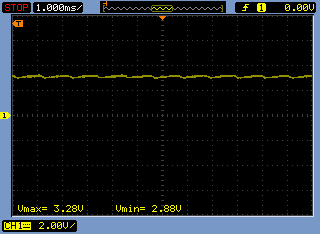
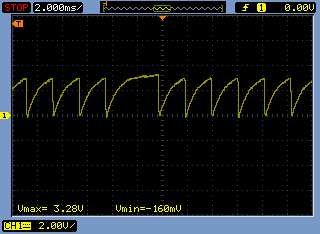
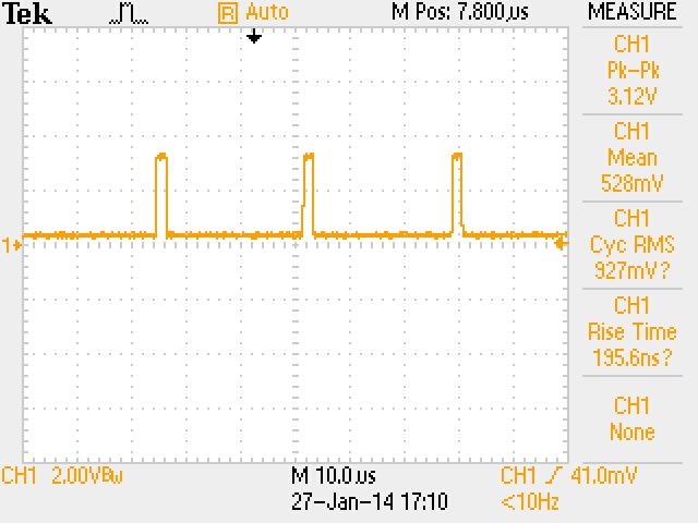
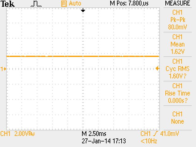
For the reset pin I was also doubtful so I soldered the pinout board for KL05 and checked for the reset pin there. On kl05 reset pin I got 1.64v. for the reset pin if I am not connecting any capacitor then getting the following pulse
after connecting the 1uf capacitor I am getting the following waveform
Now what you suggest me to do ? These voltages are when multilink is not connected to the uc. even after connecting the same results exist. These waveforms are common for both k20 and kl05 uc.
Regards
Amit Kumar
