- Forums
- Product Forums
- General Purpose MicrocontrollersGeneral Purpose Microcontrollers
- i.MX Forumsi.MX Forums
- QorIQ Processing PlatformsQorIQ Processing Platforms
- Identification and SecurityIdentification and Security
- Power ManagementPower Management
- Wireless ConnectivityWireless Connectivity
- RFID / NFCRFID / NFC
- Advanced AnalogAdvanced Analog
- MCX Microcontrollers
- S32G
- S32K
- S32V
- MPC5xxx
- Other NXP Products
- S12 / MagniV Microcontrollers
- Powertrain and Electrification Analog Drivers
- Sensors
- Vybrid Processors
- Digital Signal Controllers
- 8-bit Microcontrollers
- ColdFire/68K Microcontrollers and Processors
- PowerQUICC Processors
- OSBDM and TBDML
- S32M
- S32Z/E
-
- Solution Forums
- Software Forums
- MCUXpresso Software and ToolsMCUXpresso Software and Tools
- CodeWarriorCodeWarrior
- MQX Software SolutionsMQX Software Solutions
- Model-Based Design Toolbox (MBDT)Model-Based Design Toolbox (MBDT)
- FreeMASTER
- eIQ Machine Learning Software
- Embedded Software and Tools Clinic
- S32 SDK
- S32 Design Studio
- GUI Guider
- Zephyr Project
- Voice Technology
- Application Software Packs
- Secure Provisioning SDK (SPSDK)
- Processor Expert Software
- Generative AI & LLMs
-
- Topics
- Mobile Robotics - Drones and RoversMobile Robotics - Drones and Rovers
- NXP Training ContentNXP Training Content
- University ProgramsUniversity Programs
- Rapid IoT
- NXP Designs
- SafeAssure-Community
- OSS Security & Maintenance
- Using Our Community
-
- Cloud Lab Forums
-
- Knowledge Bases
- ARM Microcontrollers
- i.MX Processors
- Identification and Security
- Model-Based Design Toolbox (MBDT)
- QorIQ Processing Platforms
- S32 Automotive Processing Platform
- Wireless Connectivity
- CodeWarrior
- MCUXpresso Suite of Software and Tools
- MQX Software Solutions
- RFID / NFC
- Advanced Analog
-
- NXP Tech Blogs
- Home
- :
- General Purpose Microcontrollers
- :
- Kinetis Microcontrollers
- :
- KV56: Trigger HSADC with PDB
KV56: Trigger HSADC with PDB
- Subscribe to RSS Feed
- Mark Topic as New
- Mark Topic as Read
- Float this Topic for Current User
- Bookmark
- Subscribe
- Mute
- Printer Friendly Page
- Mark as New
- Bookmark
- Subscribe
- Mute
- Subscribe to RSS Feed
- Permalink
- Report Inappropriate Content
Hello,
There does not seem to be an example to trigger HSADC with the PDB. In my application I want to time a 4kHz frequency with the PDB to trigger the HSADC every 250us and then delay the sampling for 2.7us to avoid catching switching currents in my ADC read. With the normal 16 bit ADCs this is possible. However, I cannot change my board layout to map to this 16 bit ADC due to doing a chip swap between KV31 and KV56.
How would I trigger the HSADC with the PDB? Do you have an example?
Currently I have the PDB configured as below (note a modified my KV31 code and just changed the ADC hw trigger source)
void InitPDB(void)
{
CLOCK_EnableClock(kCLOCK_Pdb0);
/* Configure PDB SC register */
/* Select trigger */
/* PDB error interrupt enable */
/* PDB enable */
/* Mod and ChnDlym values will be updated from buffer by writing LDOK bit */
PDB0->SC = (PDB_SC_PDBEN_MASK | PDB_SC_LDMOD(0) | PDB_SC_TRGSEL(8) | PDB_SC_PDBEIE_MASK | PDB_SC_PRESCALER(1) );
/* Force PDB to have maximum modulus value, it will be reset by PWM */
PDB0->MOD = (g_sClockSetup.ui16M1PwmModulo * M1_FOC_FREQ_VS_PWM_FREQ - g_sClockSetup.ui16M1PwmModulo / 2);
PDB0->IDLY = (g_sClockSetup.ui16M1PwmModulo * M1_FOC_FREQ_VS_PWM_FREQ - g_sClockSetup.ui16M1PwmModulo / 2);
/* Enable channel 0, pretrigger 0 - ADC0_RA */
/* Enable channel 0, pretrigger 1 - ADC0_RB */
/* PDB Channel Back-to-back Disabled */
/* PDB Channel Pre-Trigger Enable */
/* PDB Channel Pre-Trigger Output Select */
PDB0->CH[0].C1 = (PDB_C1_EN(3) | PDB_C1_TOS(3) | PDB_C1_BB(0));
/* Enable channel 1, pretrigger 0 - ADC1_RA */
/* Enable channel 1, pretrigger 1 - ADC1_RB */
/* PDB Channel Back-to-back Disabled */
/* PDB Channel Pre-Trigger Enable */
/* PDB Channel Pre-Trigger Output Select */
PDB0->CH[1].C1 = (PDB_C1_EN(3) | PDB_C1_TOS(3) | PDB_C1_BB(0));
/* Set amount of delay for the A and B Samples */
/* This delays the ADC read after the fast thread timing has been counted */
/* We need to delay the ADC read so that we don't catch the low side IGBT switching on current spike */
/* Center aligned PWM keeps ADC reads at optimal location when PWM is low */
/* DLY0 = (0.4us / PWM_TS) * PDB0_MOD, DLY1 = (2.7us / PWM_TS) * PDB0_MOD */
/* ADC samples take 2.7us so delays need to be in increments of 2.7us */
PDB0->CH[0].DLY[0] = 45; // 2.7us
PDB0->CH[0].DLY[1] = 90; // 5.4us
PDB0->CH[1].DLY[0] = 45; // 2.7us
PDB0->CH[1].DLY[1] = 90; // 5.4us
/* Load values */
PDB0->SC |= PDB_SC_LDOK_MASK;
/* Configure SIM for ADC hw trigger source PDB */
SIM->SOPT7 &= ~(SIM_SOPT7_HSADC0AALTTRGEN_MASK | SIM_SOPT7_HSADC0BTRGSEL_MASK | SIM_SOPT7_HSADC1ATRGSEL_MASK | SIM_SOPT7_HSADC1BTRGSEL_MASK);
/* Enable & setup interrupts */
EnableIRQ(PDB0_IRQn);
NVIC_SetPriority(PDB0_IRQn, 13);
// Start PDB
PDB_Enable(PDB0, true);
}
However, I don't see an option for a hardware trigger on an HSADC to pass into HSADC_EnableInterrupts()?
Solved! Go to Solution.
- Mark as New
- Bookmark
- Subscribe
- Mute
- Subscribe to RSS Feed
- Permalink
- Report Inappropriate Content
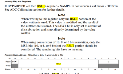
I think I figured this out - my ADC was only reading 0 to 0.38V and then rolling over. The problem was that I did not realize the format of the RESULT register:
The ADC conversion is shifted left by 3 bits. Therefore, I need to shift the value right by 3 bits to read 12 bit 0 to 4095 number.
- Mark as New
- Bookmark
- Subscribe
- Mute
- Subscribe to RSS Feed
- Permalink
- Report Inappropriate Content
Hi Derek Cook,
An apology for the late reply and thank you so much for using our community.
Unfortunately, we do not have an example of triggering HSADC via PDB. However, regarding to your question, you need to use HSADC_EnableConverterSyncInput to select hardware trigger.
On the other hand, another option is to trigger HSADC via PDC using XBARA connections instead of SIM_SOPT7.
I hope this will help you. Please let me know if you have more questions about it.
- Mark as New
- Bookmark
- Subscribe
- Mute
- Subscribe to RSS Feed
- Permalink
- Report Inappropriate Content
Thanks for the reply! I have my hardware now and I'll let you know if I run into any issues.
- Mark as New
- Bookmark
- Subscribe
- Mute
- Subscribe to RSS Feed
- Permalink
- Report Inappropriate Content
I'm having a little trouble with the HSADC. What I am trying to do is use HSADC0 and HSADC1 to get 2 simultaneous conversions on each ADC running both ADCs at the same time to get 4 simultaneous conversions.
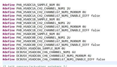
I followed the demo twrkv58f220m_hsadc_dual_parallel_conversion. The only difference I made was that I am using both HSADCs and also I don't want differential conversions so I have enableDifferentialPair false on each channel.
This is my setup:
/* enable clock for ADC0 and HS ADC modules modules*/
CLOCK_EnableClock(kCLOCK_Adc0);
CLOCK_EnableClock(kCLOCK_Hsadc0);
CLOCK_EnableClock(kCLOCK_Hsadc1);
/* Initialize the HSADC common digital control.
* "kHSADC_DualConverterWorkAsTriggeredParallel" and simultaneous mode is used in this case. The two conversion
* sequence would be executed by each converter at the same time. Both converter shares the converter A's control
* logic such as start, stop, DMA enable, sync input etc.
*/
HSADC_GetDefaultConfig(&hsadcConfigStruct);
HSADC_Init(HSADC0_BASEADDR, &hsadcConfigStruct);
HSADC_Init(HSADC1_BASEADDR, &hsadcConfigStruct);
/* Configure each converter. */
HSADC_GetDefaultConverterConfig(&hsadcConverterConfigStruct);
/* Enable the calibration in power up period. */
hsadcConverterConfigStruct.powerUpCalibrationModeMask = (kHSADC_CalibrationModeSingleEnded);
HSADC_SetConverterConfig(HSADC0_BASEADDR, kHSADC_ConverterA | kHSADC_ConverterB, &hsadcConverterConfigStruct);
HSADC_SetConverterConfig(HSADC1_BASEADDR, kHSADC_ConverterA | kHSADC_ConverterB, &hsadcConverterConfigStruct);
/* Enable the power for each converter. */
HSADC_EnableConverterPower(HSADC0_BASEADDR, kHSADC_ConverterA | kHSADC_ConverterB, true);
HSADC_EnableConverterPower(HSADC1_BASEADDR, kHSADC_ConverterA | kHSADC_ConverterB, true);
while (
(kHSADC_ConverterAPowerDownFlag | kHSADC_ConverterBPowerDownFlag) ==
((kHSADC_ConverterAPowerDownFlag | kHSADC_ConverterBPowerDownFlag) & HSADC_GetStatusFlags(HSADC0_BASEADDR)))
{
}
while (
(kHSADC_ConverterAPowerDownFlag | kHSADC_ConverterBPowerDownFlag) ==
((kHSADC_ConverterAPowerDownFlag | kHSADC_ConverterBPowerDownFlag) & HSADC_GetStatusFlags(HSADC1_BASEADDR)))
{
}
/* Wait the calibration process complete. None End of Scan flag will be set after power up calibration process. */
while ((kHSADC_ConverterAEndOfCalibrationFlag | kHSADC_ConverterBEndOfCalibrationFlag) !=
((kHSADC_ConverterAEndOfCalibrationFlag | kHSADC_ConverterBEndOfCalibrationFlag) &
HSADC_GetStatusFlags(HSADC0_BASEADDR)))
{
}
while ((kHSADC_ConverterAEndOfCalibrationFlag | kHSADC_ConverterBEndOfCalibrationFlag) !=
((kHSADC_ConverterAEndOfCalibrationFlag | kHSADC_ConverterBEndOfCalibrationFlag) &
HSADC_GetStatusFlags(HSADC1_BASEADDR)))
{
}
HSADC_ClearStatusFlags(HSADC0_BASEADDR,
(kHSADC_ConverterAEndOfCalibrationFlag | kHSADC_ConverterBEndOfCalibrationFlag));
HSADC_ClearStatusFlags(HSADC1_BASEADDR,
(kHSADC_ConverterAEndOfCalibrationFlag | kHSADC_ConverterBEndOfCalibrationFlag));
/* Make each converter exit stop mode. */
HSADC_EnableConverter(HSADC0_BASEADDR, kHSADC_ConverterA | kHSADC_ConverterB, true);
HSADC_EnableConverter(HSADC1_BASEADDR, kHSADC_ConverterA | kHSADC_ConverterB, true);
ConfigureFastADCSamples();
void ConfigureFastADCSamples(void)
{
/* Configure the samples. */
HSADC_GetDefaultSampleConfig(&hsadcSampleConfigStruct);
/* For converter HSADC0 Conv A. */
hsadcSampleConfigStruct.channelNumber = DCBUSV_HSADC0A_CH6_CHANNEL_NUM1;
hsadcSampleConfigStruct.channel67MuxNumber = DCBUSV_HSADC0A_CH6_CHANNEL67_NUM1_MUXNUM;
hsadcSampleConfigStruct.enableDifferentialPair = DCBUSV_HSADC0A_CH6_CHANNEL67_NUM1_ENABLE_DIFF;
HSADC_SetSampleConfig(HSADC0_BASEADDR, DCBUSV_HSADC0A_SAMPLE_NUM, &hsadcSampleConfigStruct);
/* For converter HSADC0 Conv B. */
/* For converter B.
* In HSADC_SetSampleConfig(), the channel number 0~7 represents input 0~7 of converter A and channel number 8~15
* represents input 0~7 of converter B.
*/
hsadcSampleConfigStruct.channelNumber = (PHC_HSADC0B_CH2_CHANNEL_NUM1 + 8U);
hsadcSampleConfigStruct.channel67MuxNumber = PHC_HSADC0B_CH2_CHANNEL67_NUM1_MUXNUM;
hsadcSampleConfigStruct.enableDifferentialPair = PHC_HSADC0B_CH2_CHANNEL67_NUM1_ENABLE_DIFF;
HSADC_SetSampleConfig(HSADC0_BASEADDR, PHC_HSADC0B_SAMPLE_NUM, &hsadcSampleConfigStruct);
/* For converter HSADC1 Conv A. */
hsadcSampleConfigStruct.channelNumber = PHA_HSADC1A_CH2_CHANNEL_NUM1;
hsadcSampleConfigStruct.channel67MuxNumber = PHA_HSADC1A_CH2_CHANNEL67_NUM1_MUXNUM;
hsadcSampleConfigStruct.enableDifferentialPair = PHA_HSADC1A_CH2_CHANNEL67_NUM1_ENABLE_DIFF;
HSADC_SetSampleConfig(HSADC1_BASEADDR, PHA_HSADC1A_SAMPLE_NUM, &hsadcSampleConfigStruct);
/* For converter HSADC1 Conv B. */
/* For converter B.
* In HSADC_SetSampleConfig(), the channel number 0~7 represents input 0~7 of converter A and channel number 8~15
* represents input 0~7 of converter B.
*/
hsadcSampleConfigStruct.channelNumber = (PHB_HSADC1B_CH2_CHANNEL_NUM1 + 8U);
hsadcSampleConfigStruct.channel67MuxNumber = PHB_HSADC1B_CH2_CHANNEL67_NUM1_MUXNUM;
hsadcSampleConfigStruct.enableDifferentialPair = PHB_HSADC1B_CH2_CHANNEL67_NUM1_ENABLE_DIFF;
HSADC_SetSampleConfig(HSADC1_BASEADDR, PHB_HSADC1B_SAMPLE_NUM, &hsadcSampleConfigStruct);
/* Enable the sample slot. */
uint16_t sampleMask = HSADC_SAMPLE_MASK(0U) /* For converter A. */
| HSADC_SAMPLE_MASK(8U); /* For converter B. */
HSADC_EnableSample(HSADC0_BASEADDR, sampleMask, true);
HSADC_EnableSample(HSADC0_BASEADDR, (uint16_t)(~sampleMask), false); /* Disable other sample slots. */
HSADC_EnableSample(HSADC1_BASEADDR, sampleMask, true);
HSADC_EnableSample(HSADC1_BASEADDR, (uint16_t)(~sampleMask), false); /* Disable other sample slots. */
}
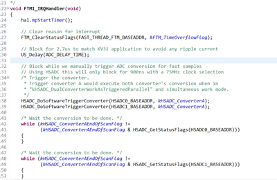
I have a FTM keeping a 250us interrupt for me and am kicking off the ADC conversion there:
Then to read ADCs I am doing this:
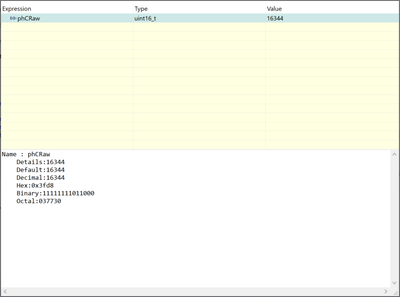
Do you see anything wrong I did in the setup? What is strange is that these are 12 bit ADCs and I seem to be getting a 16 bit number returned from the function:
- Mark as New
- Bookmark
- Subscribe
- Mute
- Subscribe to RSS Feed
- Permalink
- Report Inappropriate Content
I think I figured this out - my ADC was only reading 0 to 0.38V and then rolling over. The problem was that I did not realize the format of the RESULT register:
The ADC conversion is shifted left by 3 bits. Therefore, I need to shift the value right by 3 bits to read 12 bit 0 to 4095 number.
- Mark as New
- Bookmark
- Subscribe
- Mute
- Subscribe to RSS Feed
- Permalink
- Report Inappropriate Content
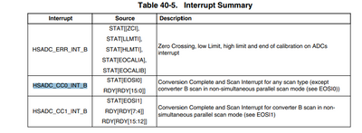
I don't even see mention of a hardware interrupt option.
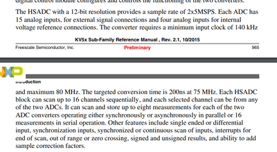
Worst case I can use PDB to trigger an interrupt on ADC0 and then in the ADC0_IRQHandler I can manually do my HSADC conversions I need. If the sample time is 200ns with 75MHz input clock this is not a big deal. I really don't even need the PDB at this point - I could use an FTM to trigger a 250us interrupt

