- Forums
- Product Forums
- General Purpose MicrocontrollersGeneral Purpose Microcontrollers
- i.MX Forumsi.MX Forums
- QorIQ Processing PlatformsQorIQ Processing Platforms
- Identification and SecurityIdentification and Security
- Power ManagementPower Management
- Wireless ConnectivityWireless Connectivity
- RFID / NFCRFID / NFC
- Advanced AnalogAdvanced Analog
- MCX Microcontrollers
- S32G
- S32K
- S32V
- MPC5xxx
- Other NXP Products
- S12 / MagniV Microcontrollers
- Powertrain and Electrification Analog Drivers
- Sensors
- Vybrid Processors
- Digital Signal Controllers
- 8-bit Microcontrollers
- ColdFire/68K Microcontrollers and Processors
- PowerQUICC Processors
- OSBDM and TBDML
- S32M
- S32Z/E
-
- Solution Forums
- Software Forums
- MCUXpresso Software and ToolsMCUXpresso Software and Tools
- CodeWarriorCodeWarrior
- MQX Software SolutionsMQX Software Solutions
- Model-Based Design Toolbox (MBDT)Model-Based Design Toolbox (MBDT)
- FreeMASTER
- eIQ Machine Learning Software
- Embedded Software and Tools Clinic
- S32 SDK
- S32 Design Studio
- GUI Guider
- Zephyr Project
- Voice Technology
- Application Software Packs
- Secure Provisioning SDK (SPSDK)
- Processor Expert Software
- Generative AI & LLMs
-
- Topics
- Mobile Robotics - Drones and RoversMobile Robotics - Drones and Rovers
- NXP Training ContentNXP Training Content
- University ProgramsUniversity Programs
- Rapid IoT
- NXP Designs
- SafeAssure-Community
- OSS Security & Maintenance
- Using Our Community
-
- Cloud Lab Forums
-
- Knowledge Bases
- ARM Microcontrollers
- i.MX Processors
- Identification and Security
- Model-Based Design Toolbox (MBDT)
- QorIQ Processing Platforms
- S32 Automotive Processing Platform
- Wireless Connectivity
- CodeWarrior
- MCUXpresso Suite of Software and Tools
- MQX Software Solutions
- RFID / NFC
- Advanced Analog
-
- NXP Tech Blogs
- Home
- :
- 通用微控制器
- :
- Kinetis微控制器
- :
- Re: FTM2 CH0 to generate simple clock of 16khz
FTM2 CH0 to generate simple clock of 16khz
FTM2 CH0 to generate simple clock of 16khz
Hi,
I am trying to generate a simple clock of 16khz using a FTM2 CH0 and below is my initialization code
void startClock() //FTM2 CH0 16khz
{
	/**********************************************************************************
	 * PORT SETUP
	 * ********************************************************************************
	 */

	// System Clock Gating Control Register 5 (SIM_SCGC5), switch on clock for port B
	*(volatile unsigned long *)(SIM_BLOCK + SIM_PORT_CLK_GATE_OFFSET) |= 0x400;

    // FTM2_CH0 on PTB18 (alt. function 3) and high drive strength
    *(volatile unsigned long *)(PORTB_BLOCK + 0x48) |= (0x00000300 | 0x00000040);

 	/**********************************************************************************
 	 * Flex Timer 2 Channel 0 Setup
 	 * ********************************************************************************
 	 */

 	// FTM2. Ensure that the FlexTimer/TPM module is powered up
     *(volatile unsigned long *)(SIM_BLOCK + 0x103c) |= 0x4000000;

    // FTM Status And Control (FTM0_SC). Disable FTM2 operation (system clock)
    *(volatile unsigned long *)(FTM2_BASE_ADDR + 0x000) = 0x00000000;

    // Configuration (FTMx_CONF) pp 1020
    // pin
    // 6 - 7 - BDM mode 3 - 0xc0 (allow timer to continue operating when debugging)
    // 9     - Enable use of global timebase from another FTM module 0x200 (Unused here)
    // 10 	 - Enable output of global timebase to other FTMs 0x400 (unused here)
    *(unsigned long *)(FTM2_BASE_ADDR + 0x084) = (0x000000c0);

    // Disable Write protection on the FTMx_MODE.
    *(unsigned long *)(FTM2_BASE_ADDR + 0x054) = 0x00000004;

    // Features Mode Selection (FTMx_MODE)
    // Switch off the enhanced FTM features to avoid needing to do an explicit software load of the CnV regs.
    // Keep write protection disabled - 0x04
    *(unsigned long *)(FTM2_BASE_ADDR + 0x054) = (0x00000004 | 0x0000000);

    // Synchronisation (FTMx_SYNC).
    // Enable loading at maximum (i.e. CV == MOD) - 0x00000002
    // Software triggering is enabled - 0x80
    *(unsigned long *)(FTM2_BASE_ADDR + 0x58) = (0x00000002 | 0x80);

    // Set counter MOD register to the value that provides the frequency of interest.
    // 0x3C6  - 1 kHz with a pre-scaler of 128
    // 0x0BB; - 320 kHz
    *(unsigned long *)(FTM2_BASE_ADDR + FTM2_MOD) =  3750-1;//0x0BB;// - 320 kHz;

    // Synchronisation Configuration (FTMx_SYNCONF)
    // set SYNCMODE (Enhanced PWM synchronisation is selected.) - 0x80
    // set SWRSTCNT = 1 (FTM counter synchronisation is activated by the software trigger) - 0x100
    // set SWWRBUF = 1 (MOD, CNTIN, and CV registers synchronisation is activated by the software trigger.) - 0x200
    *(unsigned long *)(FTM2_BASE_ADDR + 0x8C) = (0x200);

    // Channel (n) Status And Control (FTMx_CnSC)
    // ELSnB:ELSnA = 1:0 Edge-Aligned PWM High-true pulses (clear Output on match) - 0x08
    // MSnB:MSnA = 1:0 (See ELSnB:ELSnA) - 0x20
    *(volatile unsigned long *)(FTM2_BASE_ADDR + FTM2_C0SC_OFFSET) = (0x00000020 | 0x00000008);

    // Set counter initial value to zero
    *(volatile unsigned long *)(FTM2_BASE_ADDR + 0x04c) = 0;
    *(volatile unsigned long *)(FTM2_BASE_ADDR + 0x060) = 0x01;
    // prepare first PWM value (place it in the CnV register)
    *(volatile unsigned long *)(FTM2_BASE_ADDR + FTM2_C0V_OFFSET) = 3750/2;//0x5D;//0x1E3;
}
I am generating an SPWM on FTM0 CH6 and 7 too, so I am enabling both the FTM modules together after initializing the FTM0 module as below.
     /**********************************************************************************
   * Enable Clock to FTM module.
   * ********************************************************************************
   */

     // FTM Status And Control (FTM0_SC). Enable FTM0 operation (system clock)
     *(volatile unsigned long *)(FTM0_BASE_ADDR + 0x000) = 0x00000008;
    // FTM Status And Control (FTM2_SC). Enable FTM2 operation (system clock)
     *(volatile unsigned long *)(FTM2_BASE_ADDR + 0x000) = 0x00000008;
I am getting the SPWM output on PTA 1/2 but the FTM2 clock output on PTB18 isn't getting generated. The output is turned ON and OFF using GPIOB Pin 19.
Is there some settings that are missing in the above code? I have enabled the clock to PORTB & PORTA in board init.
Regards,
Rashmitha
Hi,
Did you get this to work?
If you weren't aware, NXP supplies header files for each of the Kinetis processor series, so you don't need to hard-code the base offsets.
I don't see an immediate problem in your code, but I would leave out everything regarding synchronization, when all you want to do is to generate a PWM at 16 kHz and 50% duty cycle.
I would also re-arrange the order a bit, so that the channel specific stuff is the first thing that is defined. Otherwise, the following is pretty much how you already configure the FTM2.
// Set FTM mode to edge-aligned PWM, clear output on match.
FTM2->CONTROLS[0].CnSC = FTM_CnSC_MSB_MASK | FTM_CnSC_ELSB_MASK;
FTM2->CONTROLS[0].CnV = 3750/2;

// Ensure that write protection of FTM_SC_REG is off (it always should be).
FTM2->MODE |= FTM_MODE_WPDIS_MASK;
// Make sure we are using legacy (non-FTM) behavior. This should be default,
// but is important to meet buffered updates of FTM_CnV_REG, as mentioned in Sec. 38.4.10.3. (MK22FN256VLL12 user manual)
FTM2->MODE &= ~FTM_MODE_FTMEN_MASK;
// Make sure that FTM (PWM) is running in JTAG/debug modes as well.
FTM2->CONF = FTM_CONF_BDMMODE(3);
// Load MOD (modulus) or overflow value. This is the PWM freq which applies across the whole FTM2 module.
FTM2->MOD = 3750;
// Reset counter value
FTM2->CNT = 0;
// Reset initial counter value. This is also reset by selecting a clock source in FTM_SC_CLKS.
// Must always be 0 for EPWM (Sec. 38.4.6)
FTM2->CNTIN = 0;
// Enable FTM with bus clock with no prescaler.
FTM2->SC = FTM_SC_CLKS(1) | FTM_SC_PS(0);
Hope this helps.
Kind regards,
Troels
Dear Rashmitha,
Thank you so much for your patience, please check this information below, I hope it be useful:
I truly recommend download and install MCUXpresso IDE,
Once installed you can import examples about FTM in your IDE to debug and run it on your development board.
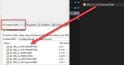
Download the following SDK: Dashboard | MCUXpresso SDK Builder (nxp.com)
- To install drag and drop the file in MCUXpresso installed SDKs section, please see the picture.
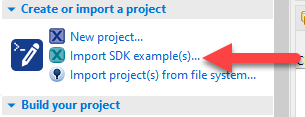
- Create new project, please press this option.
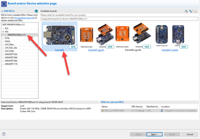
- Select the correct board then press next.
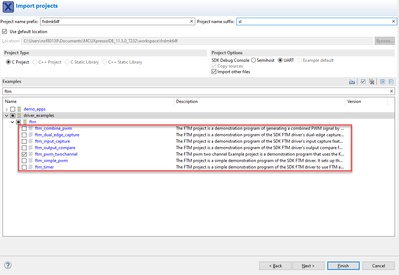
- You will be able to find different kind of examples about FTM.
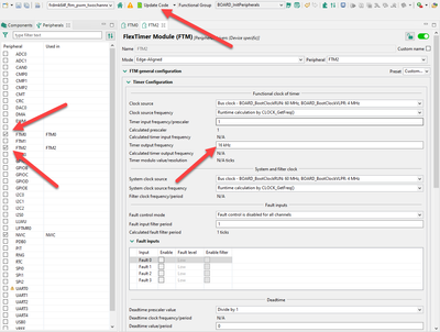
When you get at this point, you can enable FTM2 with your clock preferences, just follow the next steps:
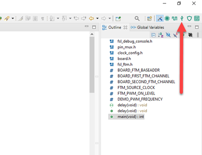
- Please click in peripherals, it is right top in screen:
- Enable peripherals as in the picture if its needed then close.
- Left side please select the FTM you want to enable and choose clock frecuency, then press Update Code button, this will generate code to enable the FTM as you want.
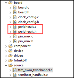
Last step is consult the generated code in the following files then you can use them in the main file called “ftm_pwm_twochannel.c”.
I hope this information be useful, please let me know for any other question.
Best Regards.
-Ramon.
