- Forums
- Product Forums
- General Purpose MicrocontrollersGeneral Purpose Microcontrollers
- i.MX Forumsi.MX Forums
- QorIQ Processing PlatformsQorIQ Processing Platforms
- Identification and SecurityIdentification and Security
- Power ManagementPower Management
- Wireless ConnectivityWireless Connectivity
- RFID / NFCRFID / NFC
- Advanced AnalogAdvanced Analog
- MCX Microcontrollers
- S32G
- S32K
- S32V
- MPC5xxx
- Other NXP Products
- S12 / MagniV Microcontrollers
- Powertrain and Electrification Analog Drivers
- Sensors
- Vybrid Processors
- Digital Signal Controllers
- 8-bit Microcontrollers
- ColdFire/68K Microcontrollers and Processors
- PowerQUICC Processors
- OSBDM and TBDML
- S32M
- S32Z/E
-
- Solution Forums
- Software Forums
- MCUXpresso Software and ToolsMCUXpresso Software and Tools
- CodeWarriorCodeWarrior
- MQX Software SolutionsMQX Software Solutions
- Model-Based Design Toolbox (MBDT)Model-Based Design Toolbox (MBDT)
- FreeMASTER
- eIQ Machine Learning Software
- Embedded Software and Tools Clinic
- S32 SDK
- S32 Design Studio
- GUI Guider
- Zephyr Project
- Voice Technology
- Application Software Packs
- Secure Provisioning SDK (SPSDK)
- Processor Expert Software
- Generative AI & LLMs
-
- Topics
- Mobile Robotics - Drones and RoversMobile Robotics - Drones and Rovers
- NXP Training ContentNXP Training Content
- University ProgramsUniversity Programs
- Rapid IoT
- NXP Designs
- SafeAssure-Community
- OSS Security & Maintenance
- Using Our Community
-
- Cloud Lab Forums
-
- Knowledge Bases
- ARM Microcontrollers
- i.MX Processors
- Identification and Security
- Model-Based Design Toolbox (MBDT)
- QorIQ Processing Platforms
- S32 Automotive Processing Platform
- Wireless Connectivity
- CodeWarrior
- MCUXpresso Suite of Software and Tools
- MQX Software Solutions
- RFID / NFC
- Advanced Analog
-
- NXP Tech Blogs
- Home
- :
- General Purpose Microcontrollers
- :
- Kinetis Microcontrollers
- :
- Re: FTM CnV Update Problem
FTM CnV Update Problem
- Subscribe to RSS Feed
- Mark Topic as New
- Mark Topic as Read
- Float this Topic for Current User
- Bookmark
- Subscribe
- Mute
- Printer Friendly Page
- Mark as New
- Bookmark
- Subscribe
- Mute
- Subscribe to RSS Feed
- Permalink
- Report Inappropriate Content
So, I was trying to change the value of CnV based on the data's bit value
but the output stays in the initial wrote value but not changing
since I am just getting started in this MicroController MKE02Z64VLC4,
I don't know which step i am wrong, Please tell me which line is missing
#include "MKE02Z4.h"

#define FTM_MOD     24      // 25 ticks → 1.25us @ 20MHz
#define TICKS_0      7
#define TICKS_1     14

void FTM_Init(void)
{
    SIM->SCGC |= SIM_SCGC_FTM2_MASK;

    FTM2->MODE = FTM_MODE_WPDIS_MASK | FTM_MODE_FTMEN_MASK;

    FTM2->CNTIN = 0;
    FTM2->CNT   = 0;
    FTM2->MOD   = FTM_MOD;

    FTM2->CONTROLS[0].CnSC =
        FTM_CnSC_MSB_MASK |
        FTM_CnSC_ELSB_MASK;

    FTM2->CONTROLS[0].CnV = TICKS_0;

    /* ENABLE CHANNEL OUTPUT (CRITICAL) */
    FTM2->OUTMASK &= ~(1 << 0);

    /* Initial load */
    *(volatile __UINT32_TYPE__ *)0x4003A098 = 0x0021;

    FTM2->SC = FTM_SC_CLKS(1) | FTM_SC_PS(0);

    *(volatile __UINT32_TYPE__ *)0x4003A064 = 0x00;
}

static inline void wait_ftm_period(void)
{
    while(!(FTM2->SC & FTM_SC_TOF_MASK));
    FTM2->SC &= ~FTM_SC_TOF_MASK;
}

uint32_t word = 0x5555;

int main(void)
{
    FTM_Init();

    while (1)
    {
        for(int i = 0; i < 16; i++)
        {
            if (word & (1UL << i))
                *(volatile __UINT32_TYPE__ *)0x4003A010 = TICKS_1;
            else
            	*(volatile __UINT32_TYPE__ *)0x4003A010 = TICKS_0;

            /* ARM reload for next PWM cycle */
            *(volatile __UINT32_TYPE__ *)0x4003A098 = 0x0021;

            /* WAIT ONE PWM PERIOD */
            wait_ftm_period();
        }
    }
}
Solved! Go to Solution.
- Mark as New
- Bookmark
- Subscribe
- Mute
- Subscribe to RSS Feed
- Permalink
- Report Inappropriate Content
No, your understanding is wrong. I did a test, please see the result:
1) with the correct 0x0200=LDOK:
2) with the wrong 0x0020=LDOK:
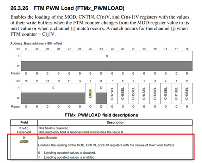
I’m afraid you’ve mixed up byte order and bit numbering. For a 32-bit register, the documentation refers to fields by bit (bit0 is the least significant, bit31 the most significant). LDOK = bit9 has nothing to do with which byte it’s in.
Hope it helps.
BR
Celeste
- Mark as New
- Bookmark
- Subscribe
- Mute
- Subscribe to RSS Feed
- Permalink
- Report Inappropriate Content
Hello @Jana_muralidharan ,
Thanks for your post.
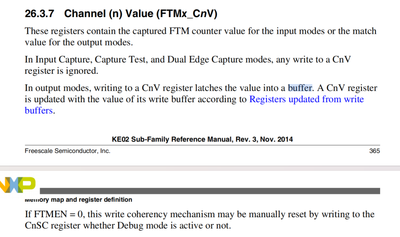
When FTMEN = 1 (which you have already set), the main registers of the FTM (including CnV, MOD, CNTIN, etc.) are write-buffered; the actual registers are only updated when a synchronization/load event is triggered. Otherwise, the new values will remain in the buffer, and the channel will continue using the old initialized values. Please see the description in RM:
Please modify the code below to set LDOK=1 to enable the load:
            /* ARM reload for next PWM cycle */
            *(volatile __UINT32_TYPE__ *)0x4003A098 = 0x0201;//0x0200=LDOK, 0x0001=CH0SEL
Hope it helps.
BR
Celeste
------------------------------------------------------------------------------------------------------------------------
Note: If this post answers your question, please click the "ACCEPT AS SOLUTION" button. Thank you!
------------------------------------------------------------------------------------------------------------------------
- Mark as New
- Bookmark
- Subscribe
- Mute
- Subscribe to RSS Feed
- Permalink
- Report Inappropriate Content
- Mark as New
- Bookmark
- Subscribe
- Mute
- Subscribe to RSS Feed
- Permalink
- Report Inappropriate Content
For this question, you can refer to our SDK demos for a deeper understanding.
Select Board | MCUXpresso SDK Builder
BR
Celeste
- Mark as New
- Bookmark
- Subscribe
- Mute
- Subscribe to RSS Feed
- Permalink
- Report Inappropriate Content
But isn't it be like this since in that register at the third byte from the left that is MSB has the LDOK not in the second right so it is the only possible thing right
0x0020=LDOK, 0x0001=CH0SEL
Isn't that right from my point of view I guess
And Thank you for replying my post 🙇🏼
And please clarify this doubt of mine too please..
- Mark as New
- Bookmark
- Subscribe
- Mute
- Subscribe to RSS Feed
- Permalink
- Report Inappropriate Content
No, your understanding is wrong. I did a test, please see the result:
1) with the correct 0x0200=LDOK:
2) with the wrong 0x0020=LDOK:
I’m afraid you’ve mixed up byte order and bit numbering. For a 32-bit register, the documentation refers to fields by bit (bit0 is the least significant, bit31 the most significant). LDOK = bit9 has nothing to do with which byte it’s in.
Hope it helps.
BR
Celeste
- Mark as New
- Bookmark
- Subscribe
- Mute
- Subscribe to RSS Feed
- Permalink
- Report Inappropriate Content
but I used the built in library's mask but still the same issue but thanks any way for your imediate response


