- Forums
- Product Forums
- General Purpose MicrocontrollersGeneral Purpose Microcontrollers
- i.MX Forumsi.MX Forums
- QorIQ Processing PlatformsQorIQ Processing Platforms
- Identification and SecurityIdentification and Security
- Power ManagementPower Management
- Wireless ConnectivityWireless Connectivity
- RFID / NFCRFID / NFC
- Advanced AnalogAdvanced Analog
- MCX Microcontrollers
- S32G
- S32K
- S32V
- MPC5xxx
- Other NXP Products
- S12 / MagniV Microcontrollers
- Powertrain and Electrification Analog Drivers
- Sensors
- Vybrid Processors
- Digital Signal Controllers
- 8-bit Microcontrollers
- ColdFire/68K Microcontrollers and Processors
- PowerQUICC Processors
- OSBDM and TBDML
- S32M
- S32Z/E
-
- Solution Forums
- Software Forums
- MCUXpresso Software and ToolsMCUXpresso Software and Tools
- CodeWarriorCodeWarrior
- MQX Software SolutionsMQX Software Solutions
- Model-Based Design Toolbox (MBDT)Model-Based Design Toolbox (MBDT)
- FreeMASTER
- eIQ Machine Learning Software
- Embedded Software and Tools Clinic
- S32 SDK
- S32 Design Studio
- GUI Guider
- Zephyr Project
- Voice Technology
- Application Software Packs
- Secure Provisioning SDK (SPSDK)
- Processor Expert Software
- Generative AI & LLMs
-
- Topics
- Mobile Robotics - Drones and RoversMobile Robotics - Drones and Rovers
- NXP Training ContentNXP Training Content
- University ProgramsUniversity Programs
- Rapid IoT
- NXP Designs
- SafeAssure-Community
- OSS Security & Maintenance
- Using Our Community
-
- Cloud Lab Forums
-
- Knowledge Bases
- ARM Microcontrollers
- i.MX Processors
- Identification and Security
- Model-Based Design Toolbox (MBDT)
- QorIQ Processing Platforms
- S32 Automotive Processing Platform
- Wireless Connectivity
- CodeWarrior
- MCUXpresso Suite of Software and Tools
- MQX Software Solutions
- RFID / NFC
- Advanced Analog
-
- NXP Tech Blogs
- Home
- :
- 製品フォーラム
- :
- デジタルシグナルコントローラ
- :
- Re: MC56F844x dflash programming
MC56F844x dflash programming
- RSS フィードを購読する
- トピックを新着としてマーク
- トピックを既読としてマーク
- このトピックを現在のユーザーにフロートします
- ブックマーク
- 購読
- ミュート
- 印刷用ページ
- 新着としてマーク
- ブックマーク
- 購読
- ミュート
- RSS フィードを購読する
- ハイライト
- 印刷
- 不適切なコンテンツを報告
Hello,
using MC56F844789. This device has Primary program/data flash memory, mapped into 0x00 0000 - 0x01 ffff & 0x02 0000 - 0x03 ffff, and also Secondary (boot) program/data flash memory, mapped into 0x06 8000 - 0x06 bfff & 0x00 8000 - 0x00 bfff.
I can program Primary program/data flash memory, when only providing flash command an address within program space range (0x00 0000 - 0x01 ffff) - programing / erasing doesn't work when providing address from aliased data space.
However, I cannot program Secondary (boot) program/data flash memory regardless if flash command is given an address from program or data space. Software has been uploaded with checkbox "always mass erase on download" and therefore data flash shall default to 32 Kbytes of data flash, No EEPROM.
Can you please advise how to program Secondary (boot) program/data flash memory from within user application?
Thanks,
Jolanta.
解決済! 解決策の投稿を見る。
- 新着としてマーク
- ブックマーク
- 購読
- ミュート
- RSS フィードを購読する
- ハイライト
- 印刷
- 不適切なコンテンツを報告
Hi, Jolanta,
Regarding the address generation, as you know that the Flash of MC56F84xxx/MC56F82xxx use the flash IP which is the same as Kinetis, the flash IP use Byte(8 bits) accessing mode, the MC56F84xxx/82xxx use half word address mode(16 bits), so the address is left shifted by ONE bit. There are program Flash and Data Flash for DSC, they are in different domain, so we use bit23 to identify the program/data flash type. But all the information are not documented in DSC reference manual. I am sorry for the inconvenience.
BR
Xiangjun Rong
- 新着としてマーク
- ブックマーク
- 購読
- ミュート
- RSS フィードを購読する
- ハイライト
- 印刷
- 不適切なコンテンツを報告
- 新着としてマーク
- ブックマーク
- 購読
- ミュート
- RSS フィードを購読する
- ハイライト
- 印刷
- 不適切なコンテンツを報告
Hi Rong,
thanks for example. It works after address of data flash to be programmed /erased is pre-processed:
*((dword *)(void *)&FTFL_FCCOB3) = (dword)(((Address - DATA_FLASH_START) << 1) | (1UL << 23));
I couldn't find this key information about address pre-processing in device reference manual. If there is such a section, and I just didn't notice it, please provide reference.
Thanks,
Jolanta.
- 新着としてマーク
- ブックマーク
- 購読
- ミュート
- RSS フィードを購読する
- ハイライト
- 印刷
- 不適切なコンテンツを報告
Hi, Jolanta,
Regarding the address generation, as you know that the Flash of MC56F84xxx/MC56F82xxx use the flash IP which is the same as Kinetis, the flash IP use Byte(8 bits) accessing mode, the MC56F84xxx/82xxx use half word address mode(16 bits), so the address is left shifted by ONE bit. There are program Flash and Data Flash for DSC, they are in different domain, so we use bit23 to identify the program/data flash type. But all the information are not documented in DSC reference manual. I am sorry for the inconvenience.
BR
Xiangjun Rong
- 新着としてマーク
- ブックマーク
- 購読
- ミュート
- RSS フィードを購読する
- ハイライト
- 印刷
- 不適切なコンテンツを報告
Hi, Jolanta,
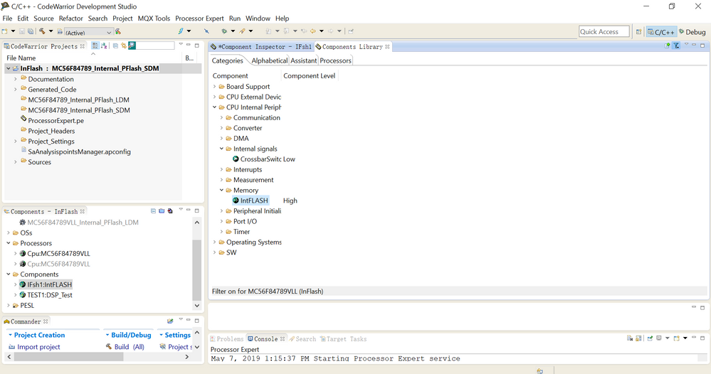
Regarding your question, we have the processor Expert(PE), the PE has intFLASH bean, with which you can erase both Program/data Flash, program Program/Data Flash.
This is the bean:
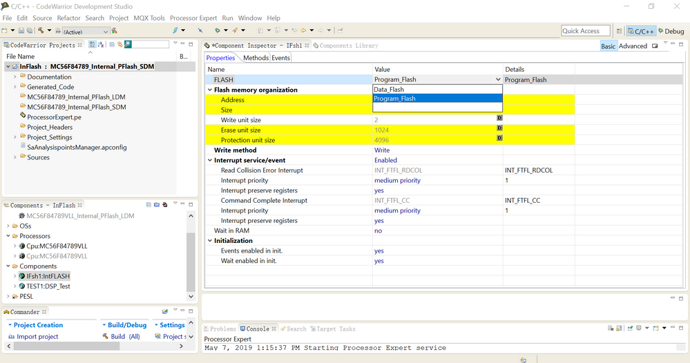
In the IntFLASH bean, you can select data Flash as Following:
I attach an example for MC56F84789 which is based on CodeWarrior for mcu ver11 tools can erase/program program flash, it tell you how to call the erasing function and program function. You can select the data flash and program it based on the erase/program function with different address and size.
Hope it can help you
BR
Xiangjun rong

