- Forums
- Product Forums
- General Purpose MicrocontrollersGeneral Purpose Microcontrollers
- i.MX Forumsi.MX Forums
- QorIQ Processing PlatformsQorIQ Processing Platforms
- Identification and SecurityIdentification and Security
- Power ManagementPower Management
- Wireless ConnectivityWireless Connectivity
- RFID / NFCRFID / NFC
- Advanced AnalogAdvanced Analog
- MCX Microcontrollers
- S32G
- S32K
- S32V
- MPC5xxx
- Other NXP Products
- S12 / MagniV Microcontrollers
- Powertrain and Electrification Analog Drivers
- Sensors
- Vybrid Processors
- Digital Signal Controllers
- 8-bit Microcontrollers
- ColdFire/68K Microcontrollers and Processors
- PowerQUICC Processors
- OSBDM and TBDML
- S32M
- S32Z/E
-
- Solution Forums
- Software Forums
- MCUXpresso Software and ToolsMCUXpresso Software and Tools
- CodeWarriorCodeWarrior
- MQX Software SolutionsMQX Software Solutions
- Model-Based Design Toolbox (MBDT)Model-Based Design Toolbox (MBDT)
- FreeMASTER
- eIQ Machine Learning Software
- Embedded Software and Tools Clinic
- S32 SDK
- S32 Design Studio
- GUI Guider
- Zephyr Project
- Voice Technology
- Application Software Packs
- Secure Provisioning SDK (SPSDK)
- Processor Expert Software
- Generative AI & LLMs
-
- Topics
- Mobile Robotics - Drones and RoversMobile Robotics - Drones and Rovers
- NXP Training ContentNXP Training Content
- University ProgramsUniversity Programs
- Rapid IoT
- NXP Designs
- SafeAssure-Community
- OSS Security & Maintenance
- Using Our Community
-
- Cloud Lab Forums
-
- Knowledge Bases
- ARM Microcontrollers
- i.MX Processors
- Identification and Security
- Model-Based Design Toolbox (MBDT)
- QorIQ Processing Platforms
- S32 Automotive Processing Platform
- Wireless Connectivity
- CodeWarrior
- MCUXpresso Suite of Software and Tools
- MQX Software Solutions
- RFID / NFC
- Advanced Analog
-
- NXP Tech Blogs
- Home
- :
- Product Forums
- :
- ColdFire/68K Microcontrollers and Processors
- :
- Re: mcf54415 sbf header and boot issue
mcf54415 sbf header and boot issue
- Subscribe to RSS Feed
- Mark Topic as New
- Mark Topic as Read
- Float this Topic for Current User
- Bookmark
- Subscribe
- Mute
- Printer Friendly Page
- Mark as New
- Bookmark
- Subscribe
- Mute
- Subscribe to RSS Feed
- Permalink
- Report Inappropriate Content
Hi all,
i am trying booting u-boot using SBF and a SPI NOR flash. I am actually flashing the spi NOR with a small tool i did running from sram.
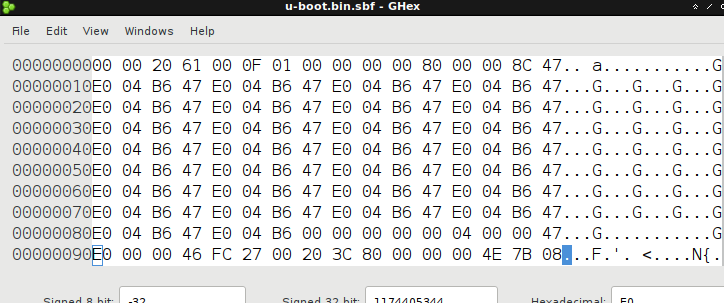
So, i program the SPI NOR with an u-boot (derived from the fsl TWR system, so same start.S) but prepending the binary with the 7 bytes of sbf header just before.
So from the above SBF header i would boot just a chunk of 32k. I see by scope 32k of data read from the SPI NOR correctly.
Btw, no code seems executed just after this load.
Is it possible this is due to some incorrect SBF_RCON setup ?
I have a 30Mhz crystal so if anyone have a sbf header i can test, as proven to work, that's welcome.
Many thanks,
angelo
Solved! Go to Solution.
- Mark as New
- Bookmark
- Subscribe
- Mute
- Subscribe to RSS Feed
- Permalink
- Report Inappropriate Content
I haven't ever done this, I'm just reading the manual. From there, the SBF bytes should be:
00 Four zero bits for sync, then 4 bits of BLDIV
00 20 0x2000 (8k longs or 32k bytes)
61 00 0F 01 0x010F0061 - 32 bit muxed, NAND, PLL Div 1, 0x0F, other dividers
==== Code Follows ====
00 00 00 00 Stack Pointer is ZERO?
80 00 00 8C Initial Program Counter in SRAM at 8000008c or 8c000000
47 E0 04 B6 These are meant to be Interrupt Vectors. Those addresses aren't in RAM?
Are you sure the BLDIV is appropriate for your clock rate? What is the SPI clock and is it "legal" for your memory chip? At least you can measure this with your scope.
I'm surprised at the above as it is reading the SPI Flash in LITTLE_ENDIAN order, and this is a BIG_ENDIAN CPU. It is documented as reading the "Length" in little-endian, so maybe it reads all the code the same way. It doesn't say at all.
If it is reading the code big-endian, then the code starts at 0x8000008C, or at "93" in your dump, which is "46FC 2700 203C 8000 0000", or:
46FC 2700 move.w #2700, %sr
203C 8000 0000 move.l #80000000, %d0 (maybe)
4EB7 jmp (somewhere)
Yes, that looks like your code. Are you sure you don't want to set up a stack pointer in the vector table? And where did those vector addresses come from? I'm guessing the bootstrap copies itself to SDRAM (0x40000000) after setting it up.
But if the SBF is reading the rest of the chip little-endian, then you code is going to end up scrambled.
Type "SBF" into the Search Bar on this page and see if anything else shows up.
If you can get a copy of a working SPI Flash image, you can disassemble it like I did to work out what order the bytes are in. Use the table in the "CFPRM.pdf" document to do this.
Make sure you get a copy of the older version of the manual. The new one has one of the chapters broken. Read here:
https://community.nxp.com/message/306792
Tom
- Mark as New
- Bookmark
- Subscribe
- Mute
- Subscribe to RSS Feed
- Permalink
- Report Inappropriate Content
Hi Tom !
thanks for the "family" support, seems we are few "lonely" coldfire cowboys now a day :smileyhappy:
SOLVED.
Ok i try to explain what happen, if some day some other developer pass from here with a similar issue.
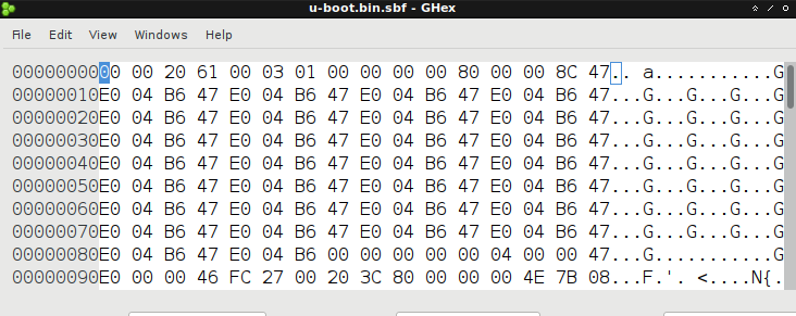
1) as Tom explained, SBF header CODE LENGTH (2 bytes) and SBF_RCON header (4 bytes), for mcf5441X,
must be written "little endian" into the SPI NOR. Strange but true :smileyhappy:
2) as Tom explained, another important thing is to set a quite low clock setup in SBF_RCON fields, or a too high clock (not supported from spi nor) screw up the program loading.
3) rest of the code can be written "as is", as produced from the compiler, so addresses are "big endian"
4) note that length must be in longwords and total code must not exceed 64KB of internal SRAM or the code in excess is anyway read and probably wrapped around that limit back to 0x80000000 screwing up the boot.
I paste here below a working sbf header for mcf54415 and a 30Mhz crytal, tested by a square wave on gpios.
still many thanks Tom,
regards,
angelo
- Mark as New
- Bookmark
- Subscribe
- Mute
- Subscribe to RSS Feed
- Permalink
- Report Inappropriate Content
I haven't ever done this, I'm just reading the manual. From there, the SBF bytes should be:
00 Four zero bits for sync, then 4 bits of BLDIV
00 20 0x2000 (8k longs or 32k bytes)
61 00 0F 01 0x010F0061 - 32 bit muxed, NAND, PLL Div 1, 0x0F, other dividers
==== Code Follows ====
00 00 00 00 Stack Pointer is ZERO?
80 00 00 8C Initial Program Counter in SRAM at 8000008c or 8c000000
47 E0 04 B6 These are meant to be Interrupt Vectors. Those addresses aren't in RAM?
Are you sure the BLDIV is appropriate for your clock rate? What is the SPI clock and is it "legal" for your memory chip? At least you can measure this with your scope.
I'm surprised at the above as it is reading the SPI Flash in LITTLE_ENDIAN order, and this is a BIG_ENDIAN CPU. It is documented as reading the "Length" in little-endian, so maybe it reads all the code the same way. It doesn't say at all.
If it is reading the code big-endian, then the code starts at 0x8000008C, or at "93" in your dump, which is "46FC 2700 203C 8000 0000", or:
46FC 2700 move.w #2700, %sr
203C 8000 0000 move.l #80000000, %d0 (maybe)
4EB7 jmp (somewhere)
Yes, that looks like your code. Are you sure you don't want to set up a stack pointer in the vector table? And where did those vector addresses come from? I'm guessing the bootstrap copies itself to SDRAM (0x40000000) after setting it up.
But if the SBF is reading the rest of the chip little-endian, then you code is going to end up scrambled.
Type "SBF" into the Search Bar on this page and see if anything else shows up.
If you can get a copy of a working SPI Flash image, you can disassemble it like I did to work out what order the bytes are in. Use the table in the "CFPRM.pdf" document to do this.
Make sure you get a copy of the older version of the manual. The new one has one of the chapters broken. Read here:
https://community.nxp.com/message/306792
Tom

