- Forums
- Product Forums
- General Purpose MicrocontrollersGeneral Purpose Microcontrollers
- i.MX Forumsi.MX Forums
- QorIQ Processing PlatformsQorIQ Processing Platforms
- Identification and SecurityIdentification and Security
- Power ManagementPower Management
- MCX Microcontrollers
- S32G
- S32K
- S32V
- MPC5xxx
- Other NXP Products
- Wireless Connectivity
- S12 / MagniV Microcontrollers
- Powertrain and Electrification Analog Drivers
- Sensors
- Vybrid Processors
- Digital Signal Controllers
- 8-bit Microcontrollers
- ColdFire/68K Microcontrollers and Processors
- PowerQUICC Processors
- OSBDM and TBDML
- S32M
-
- Solution Forums
- Software Forums
- MCUXpresso Software and ToolsMCUXpresso Software and Tools
- CodeWarriorCodeWarrior
- MQX Software SolutionsMQX Software Solutions
- Model-Based Design Toolbox (MBDT)Model-Based Design Toolbox (MBDT)
- FreeMASTER
- eIQ Machine Learning Software
- Embedded Software and Tools Clinic
- S32 SDK
- S32 Design Studio
- GUI Guider
- Zephyr Project
- Voice Technology
- Application Software Packs
- Secure Provisioning SDK (SPSDK)
- Processor Expert Software
- MCUXpresso Training Hub
-
- Topics
- Mobile Robotics - Drones and RoversMobile Robotics - Drones and Rovers
- NXP Training ContentNXP Training Content
- University ProgramsUniversity Programs
- Rapid IoT
- NXP Designs
- SafeAssure-Community
- OSS Security & Maintenance
- Using Our Community
-
- Cloud Lab Forums
-
- Knowledge Bases
- ARM Microcontrollers
- i.MX Processors
- Identification and Security
- Model-Based Design Toolbox (MBDT)
- QorIQ Processing Platforms
- S32 Automotive Processing Platform
- Wireless Connectivity
- CodeWarrior
- MCUXpresso Suite of Software and Tools
- MQX Software Solutions
-
- Home
- :
- NXP Tech Blog
- :
- i.MX RT600 Hardware Design – Part 1 of 3 – Package and Power
i.MX RT600 Hardware Design – Part 1 of 3 – Package and Power
i.MX RT600 Hardware Design – Part 1 of 3 – Package and Power
In my previous article series, I introduced a special member of the i.MX RT crossover family: the RT600. The RT600 is bit different from the other MCUs in the crossover family as it is focused on high-end audio processing, embedded signal processing and AI/ML applications. If you haven’t taken a look already, you can find the articles here and here.
As a real-world example, I this article is part one of several articles that will step through a basic RT600 hardware design and bring-up. I find this to be a very useful exercise as high-end MCU’s can be overwhelming, especially to those coming from a traditional MCU background. The goal here is to develop a simple “minimal configuration” example and build it for a demonstration. There are resources available to helping you design with the RT600 such as the “Hardware Development Guide for the RT600 Processor” (RT600HDUG) and the MIMXRT685-EVK. These resources can help bootstrap your next design. My personally view is that have several different perspectives available. Between the existing reference material and this article series, there should be enough information to start your next RT600 design with confidence.
The Minimal Configuration RT600 Project – Codename “Super-Monkey”
Last year, I did similar project codenamed “Mini-Monkey” using the LPC55S69 in its VFBGA98 package. It was an exercise to illustrate a simple project that using the 0.5mm VFBGA98 package on a low cost 2-layer PCB process. That hardware project demonstrated the LPC55S69 being able to do things like microphone capture, visualization and animated GIF decoding.
The RT600 definitely a “step up” from the LPC55S69 and is well suited to high end audio applications. Between the 300MHz CM33, the PowerQuad co-processor and the 600MHz ten silica HIFI4 DSP, there quite a bit of horsepower! It was obvious to me that that the RT600 could be a great fit all my future real-time DSP audio processing projects. In 2011, I built the “Active Pickguard” demonstrating what could be accomplished with the Kinetis K20 (Cortex-M4) device.
10 years later there have been some serious advances in embedded technologies. Rev 2 of the Active pickguard has been in the back of my mind for a while now and he RT600 is a potential great fit!
In order to run some experiments with the RT600 in-situ, I want to design a small module that bootstraps the RT600 with everything I need for my high-end audio applications. Since I may go through several iterations, I thought a simple module (like the Mini-Monkey) would be a good start point. To get things “out the door”, it is important to set clear boundaries at the outset. I do not need the module to bring out all the features of the RT600. The initial goal is to get the most critical IO to get my audio projects moving. Iteration is very important in the engineering process so thought I would keep it simple to keep momentum going.
Since the RT600 is a significant step up in performance from the LPC55S69 base Mini-Monkey, I thought the codename “Super-Monkey” would be good fit. It leaves me with options for future projects (hint hint!). Ultra-Monkey, Mega-Monkey, Nano-Monkey….
My Initial Specs for the RT600 Super-Monkey Module:
- IO breakout for 8 digital microphones (DMICs)
- One TDM input for up to 8-channel audio in (one flexcomm channel)
- Two separate I2S audio output channels. One will be for outputting audio and the other will be a special monitor (two flexcomm channels)
- I3C Access. This is a new feature I have been wanting to experiment.
- Header to add an optional circular TFT display.
- SWD debug access
- USB connector for ISP boot and power
- A debug UART
- A handful of GPIO
- +5v power via USB or IO pins
- On board Flash (the RT600 is a flash-less part)
- Crystal/clock management
I have not yet decided on a form-factor for the Super-Monkey. I need something to bring out all my audio IO and fit well with future pickguard designs. These types of boards tend to be artistic in nature, so I probably will not reveal the Super-Monkey form factor until at least the next article.
RT600 PCB Layout Consideration: The VFBGA176 Package
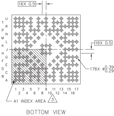
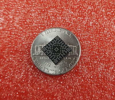
The first order of business when I approach a new hardware design is to understand the device package and any implications of the pin geometries. For the Super-Monkey project, I will be designing with the MIMXRT685SFVKB which uses the VFBGA176 package. The VFBGA176 is a 9mm x 9mm ball grid array (BGA) with 0.5mm pitch. A fine pitch BGA package can be intimidating, especially for those who may only have experience with microcontrollers in QFP packages. One of the reasons I built the “Mini-Monkey” was to demonstrate that the LPC55S69 VFBGA98 package option was doable with a 2-Layer process and low-cost design rules. The VFBGA176 was designed to be easy to fanout and is routable with a practical 4-layer process.
Figure 1. The VFBGA176 Package.
I enjoy studying unique BGA ball arrangements. This package is a work of art. Notice that this are several regions left unpopulated making it simpler to fan out. In many cases, a 0.5mm BGA would require filled micro via-in-pad to fanout the IO. There was quite a bit of thought put into the pinout of the RT600 and it is possible to fan this device out without via-in-pad technology.
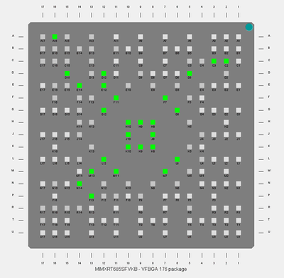
Many of the balls on the interior are VSS connections. Using the MCUXpresso pin tool, one can highlight pins to get an get a rough sense of the layout strategy.
Figure 2: Signal Highlighting with the MCUXpresso SDK Pin Tool
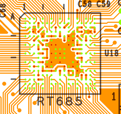
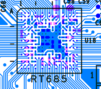
I spent some time analyzing the Gerber files from RT685EVK to get a feel for the layout. The fanout of this package is very practical.
Figure 3: RT600 VFBGA176 Fanout
Notice that *all* of the signal pads can be fanned out on the top layer. The via connections (red dots) are to connect to the power & return planes on inner layers. The vias are placed in the depopulated ball regions. The IO fanout on the RT685EVK use 4.5mil width/ 5 mil space geometry. The vias under the device package use 6mil drills. These geometries are a bit tightener than what is typical required by traditional microcontrollers, but it is well within the capabilities of many PCB fab houses. I believe the 6mil drill could possibly be increase to 8mil. The Super-Monkey will not be using all the IO and I will be targeting a 4-layer design so routing should be straightforward.
Since the only vias use in the fanout are for power and returns, there is plenty of space to place decoupling capacitors on the opposite side of the PCB. Figure 4 illustrates the placement of the decoupling caps on the RT685EVK. They are nearby existing vias to direct feed the power planes.
Figure 4: RT6600 VFBGA176 decoupling capacitor strategy
Many 0.5mil pitch BGAs require via-in-pad technology along with blind/buried stack-ups so the fanout vias do not interfere with the decoupling capacitors on the opposite side of the PCB. In the case of the VFBGA176, we can use lower cost processes as we do not need via-in-pad technology or a blind/buried stackup. Fanout and decoupling capacitor placement is straightforward for the RT600 VFBGA176 package. I really like to understand package geometry before I start a design as it can directly influence other decisions down the pipeline. The time spent analyzing the Gerbers on the RT685EVK was well spent as I now have confidence the fanout of the part will not require any exotic PCB process technology.
RT600 Power
Once I study the packaging for a new MCU, the next order of business is to understand the power supply architecture. MCU power supply design is intertwined with PCB layout strategy, so it is a good idea to understand both early in the design process.
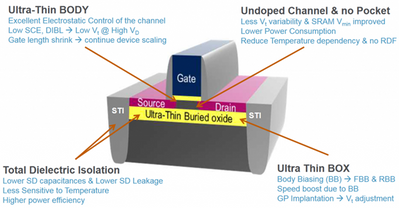
The RT600 crossover MCU power/performance ratio sits at an intersection of traditional MCUs, dedicated DSPs and application processors. To get significant clock rate improvements over traditional MCUs, the RT600 was built on 28nm FD-SOI process technology. Using 28nm process technology for an MCU is a new concept that NXP has helped pioneer.
Figure 5: 28nm FD-SOI Process technology. Image Reference.
If you remember your EE300 coursework, all the major characteristics of a MOSFET are controlled by geometry. FD-SOI process technology has many advantages, one being that we can bias the body of the MOSFETs dynamically. Body biasing give us real-time programmatic control over the MOSFET threshold voltage VTH. For MCU applications, we can move VTH up or down allowing one to increase clock frequency/performance or reduce dynamic power consumption.
From the perspective of production yield and desire increased CPU clock rates, the geometries of the transistors need to be pushed to their design rule minimums. A byproduct of small transistor geometries is a numerically small value for MOSFET VDS. For 28nm FD-SOI process technology, the nominal MOSFET VDS has been characterized to 1.0v nominal. This means the “core” logic needs powered from a 1.0v supply.
Why are many traditional MCUs powered at +3.3v?
Even though 28nm FD-SOI is 1.0v nominal, one can imagine the maximum allowed VDS to also scale up with geometry. You might not be aware, but many +3.3v MCUs might still have cores that need +1.2v, 1.8v or 2.5v core power because of the underlying process technology. The MCU will usually incorporate an LDO that the end user may not be aware of. Sometimes this internal LDO is documented in the device datasheet but it might not always be the case.
As the core voltage requirements are pushed lower, the internal LDO approach can get more inefficient resulting in additional power dissipation in the IC package. The core logic is one of the largest consumers of dynamic power resulting from of all the MOSFETS switching at a high clock frequency. As the core logic voltage requirement drops, it important to have direct access to the core power domain to directly supply power from a switching DC-DC converter. As an example, the NXP LPC55S69 is built on 40nm process technology and uses a 1.2v core. It integrates its own switching DC-DC converter to minimize active power dissipation.
Understanding the RT600 Power Supply Strategy
The RT600 has general power domains:
- +1.0v Core
- +1.8V for “Always-On” and Analog Functions
- +1.71 to +3.6v capable IO (which can be further divided into 3 distinct groups)
RT600 Core Power
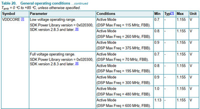
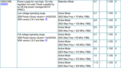
VDDCORE is used to power the internal CPU(s) and core logic. To maximize clock rate, the CPUs and core logic are constructed from the smallest transistors allowed by the process technology design rules. In the case of the RT600 and 28nm FD-SOI, the core voltage is nominally 1.0v. Looking at the RT600 datasheet, the maximum allowed value does not give one much room for error in your power supply!
It is possible to operate the core power at values than 1.0v as to save power when using lower clock frequencies. NXP provides a power library which can tune the body bias to achieve low power consumption figures at lower clock rates.
The take-away here is that by providing a separate core power supply access, the designer has flexibility in how to optimize for a particular use case. It is important to note that the RT600 include an LDO that can be powered from a +1.8v rail. Use of the LDO is not required but is available if the efficiency of a switching power supply is not required.
+1.8v “Always-On” and Analog Functions
There are several 1.8V rails in the RT600 that may be able to combine if needed. One of which is the “always-on” power domain. This domain is used for features that must be active in power down states such as the RTC, reset, optional LDO and PMIC control. In addition to the +1.8v “always-on” domain, there are +1.8v rails for other analog functions such as the ADC and comparator. +1.8v power is required for the RT600 in a minimal configuration scenario.
User IO
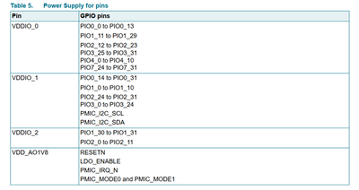
Lastly, the IO pins can be powered separately from the +1.8v functions and the core. The IO supply range is +1.71 to +3.6v with +3.3v being the most common. There are other circumstances however when you may want certain IO pins to use +1.8v. For example, many high-speed double data rate quad/octo NOR flash devices operate with a +1.8v power supply. The RT600 has 3 separate IO banks so you can have a mix of IO voltages. In a minimal configuration scenario, it would be possible to power all the IO from +1.8v reducing the number of DC-DC converters needed in a system. However, it is most likely one will require some IO at +3.3v.
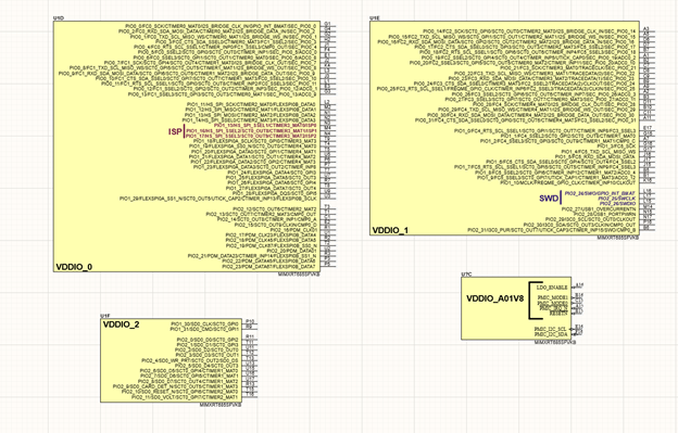
It is important to understand all the IO power options at the outset of a design. It is easy to make a mistake and end up with a non-functional part design. For my own designs, I take extra steps in the schematic entry stage to ensure success. I like to break up the schematic symbol for a part based upon a particular voltage domain. This makes design reviews much simpler as it is easier to spot a mistake. For example, reset in the RT600 is in the +1.8v “always-on” domain. Make sure it is clearly marked so you do not pull it to +3.3v!
Figure 6: RT600 IO Schematic Blocks
Power Management Options for the RT600
The power architecture for the RT600 is more complicated than a traditional single voltage rail MCU as a result of its flexibility. However, once you understand the architecture, the application design is straight forward. For example, in a minimal configuration that requires +3.3v IO, one could power the RT600 with +3.3v and +1.8v using the internal LDO for the core.
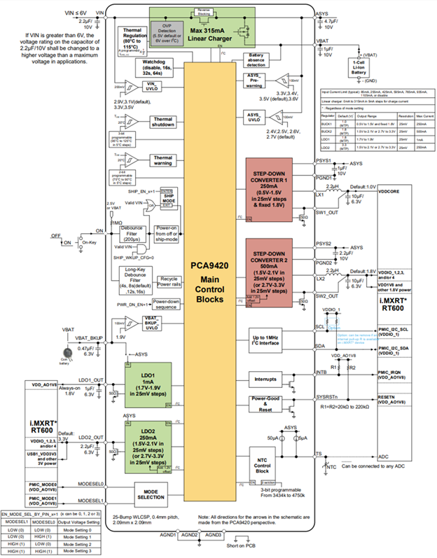
NXP offers an integrated solution that makes powering the RT600 much simpler: the PC4390 Power Management Integrated Circuit (PMIC). A PMIC is essentially a handful of DC-DC converters, LDOs and control circuitry integrated into a single package.
Figure 7: The PCA9420 PMIC
In the case of the PCA9420, it has been specifically designed to power the RT600. The out of the box configuration will perform all the necessary sequencing to bring up the device correctly. It is package in a 24-pin QFP package which is extremely compact given the number of functions it is providing. The PCA9420 also provides reset control and has an I2C interface that allows the supplies to be tuned for the different clocking configurations.
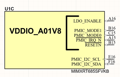
Figure 8. RT600 Dedicated PMIC Interface
I highly recommend using the PCA9420, especially if this is the first design iteration using the RT600. A designer is certainly free to use other power management solutions but the PCA9420 is a path to ensure success. If your application requires any power management and sleep functions, then the PCA9420 is an optimum choice. The Super-Monkey design will be using the PCA9420 to simplify the power supply. I plan on using the PCA9420 on the Super-Monkey as the module will powered with a single +5v rail.
The Next Steps
Power and Packaging is where I generally start designing with a new microcontroller. The RT600 parts are much more powerful than traditional microcontrollers and require a little bit more attention to detail to bring up. However, it is not as difficult as one might think, and I hope this article helped demystify the power supply and package of the RT600. There is much more information in the reference manual and hardware design guide, so I suggest that you take a look.
In my next article, I will be discussing flash memory, debug, and boot configuration on the RT600. I should also have the form-factor of the “Super-Monkey” picked out so stay tuned!
Crossing Over With the i.MX RT600 Part 1 of 2
Crossing Over With the i.MX RT600 Part 2 of 2
i.MX RT685 Hardware Design 1 of 3 - Power and Package
i.MX RT685 Hardware Design 2 of 3 - Flash Memory and Boot Configuration
i.MX RT685 Hardware Design 3 of 3 - The SuperMonkey Design
i.MX RT685 SuperMonkey QSPI Bringup with MCUXpresso and Segger J-Link
Creating a Custom Zephyr Board for the i.MX RT685 SuperMonkey
只有注册用户才能在此添加评论。 如果您已经注册,请登录。 如果您还没有注册,请注册并登录。
-
101
6 -
communication standards
4 -
General Purpose Microcontrollers
23 -
i.MX RT Processors
46 -
i.MX Processors
49 -
Interface
1 -
introduction
13 -
LPC Microcontrollers
73 -
MCUXpresso
34 -
MCUXpresso Secure Provisioning Tool
1 -
MCUXpresso Conig Tools
30 -
MCUXpresso IDE
42 -
MCUXpresso SDK
26 -
Model-Based Design Toolbox
6 -
MQX Software Solutions
2 -
QorIQ Processing Platforms
1 -
QorIQ Devices
5 -
S32N Processors
4 -
S32Z|E Processors
6 -
SW | Downloads
7 -
日本語ブログ
5
- « 前一个
- 下一个 »
