- Forums
- Product Forums
- General Purpose MicrocontrollersGeneral Purpose Microcontrollers
- i.MX Forumsi.MX Forums
- QorIQ Processing PlatformsQorIQ Processing Platforms
- Identification and SecurityIdentification and Security
- Power ManagementPower Management
- MCX Microcontrollers
- S32G
- S32K
- S32V
- MPC5xxx
- Other NXP Products
- Wireless Connectivity
- S12 / MagniV Microcontrollers
- Powertrain and Electrification Analog Drivers
- Sensors
- Vybrid Processors
- Digital Signal Controllers
- 8-bit Microcontrollers
- ColdFire/68K Microcontrollers and Processors
- PowerQUICC Processors
- OSBDM and TBDML
- S32M
-
- Solution Forums
- Software Forums
- MCUXpresso Software and ToolsMCUXpresso Software and Tools
- CodeWarriorCodeWarrior
- MQX Software SolutionsMQX Software Solutions
- Model-Based Design Toolbox (MBDT)Model-Based Design Toolbox (MBDT)
- FreeMASTER
- eIQ Machine Learning Software
- Embedded Software and Tools Clinic
- S32 SDK
- S32 Design Studio
- GUI Guider
- Zephyr Project
- Voice Technology
- Application Software Packs
- Secure Provisioning SDK (SPSDK)
- Processor Expert Software
-
- Topics
- Mobile Robotics - Drones and RoversMobile Robotics - Drones and Rovers
- NXP Training ContentNXP Training Content
- University ProgramsUniversity Programs
- Rapid IoT
- NXP Designs
- SafeAssure-Community
- OSS Security & Maintenance
- Using Our Community
-
- Cloud Lab Forums
-
- Knowledge Bases
- ARM Microcontrollers
- i.MX Processors
- Identification and Security
- Model-Based Design Toolbox (MBDT)
- QorIQ Processing Platforms
- S32 Automotive Processing Platform
- Wireless Connectivity
- CodeWarrior
- MCUXpresso Suite of Software and Tools
- MQX Software Solutions
-
- Home
- :
- i.MX论坛
- :
- i.MX RT 交叉 MCU
- :
- Re: How to access the content of the fuse map?
How to access the content of the fuse map?
The imx1060 fusemap (ref-manual chapter 22) is confusing me, so I could use some clarification...
Seems the fusemap chapter goes into a lot of detail regarding fuse addresses (ranging from 0x400 - 0x8c0) and their bits; but there is no discussion regarding how to access that address range. Then chapter 23 (OCOTP) seems to say that the OCOTP is the mechanism used to access the fuse map. Referring to the SDK's OCOTP code, I can use OCOTP_Init(), OCOTP_ReloadShadowRegister(), OCOTP_ReadFuseShadowRegister() and OCOTP_WriteFuseShadowRegister() to read/write the fuses; but I don't understand how the address passed to OCOTP_ReadFuseShadowRegister() corresponds to some entry in the fusemap.
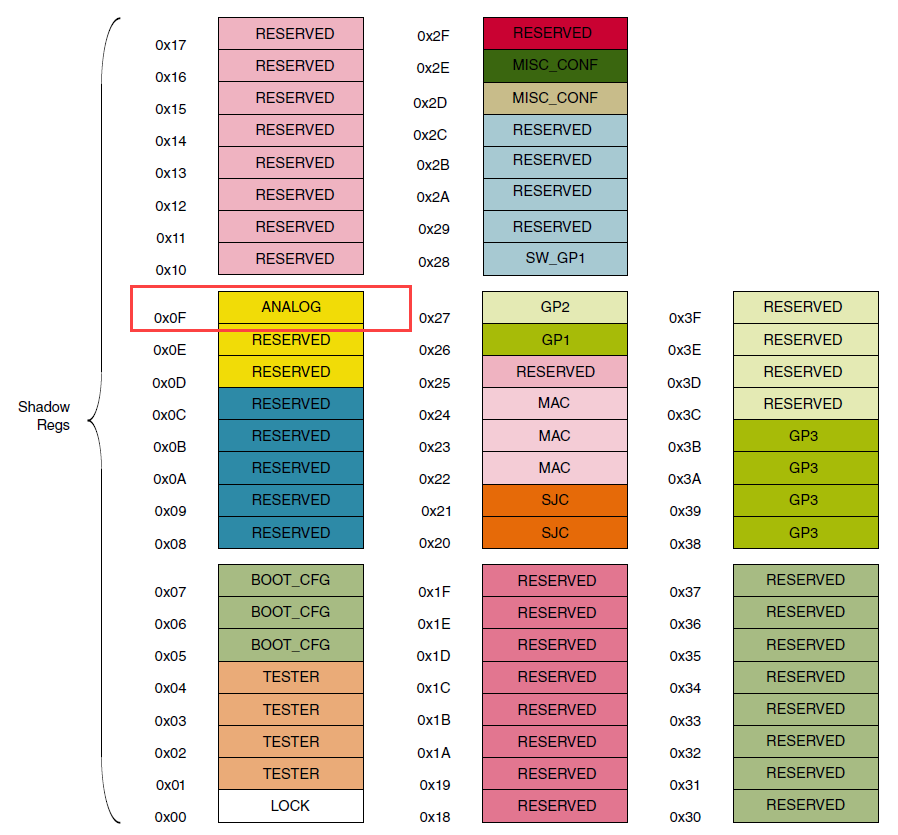
Based on the "OTP Memory Footprint" (Figure 23-2 in ref manual), there are several "not-reserved" shadow registers that can be accessed as follows:
0x00: LOCK
0x05: BOOT_CFG
0x06: BOOT_CFG
0x07: BOOT_CFG
0x0F: ANALOG
0x20: SJC
0x21: SJC
0x22: MAC
0x23: MAC
0x24: MAC
0x26: GP1
0x27: GP2
0x28: SW_GP1
0x2D: MISC_CONF
0x2E: MISC_CONF
0x38: GP3
0x39: GP3
0x3A: GP3
0x3B: GP3
Do each of these registers somehow correspond to entries fusemap? If yes, how? If no, what am I missing?
Are the functions I mention above the correct hooks into the fusemap?
已解决! 转到解答。
Hi Ed,
I think I understood your confusion. For the explanation, I will take as an example the ANALOG group that is at location 0x0F.
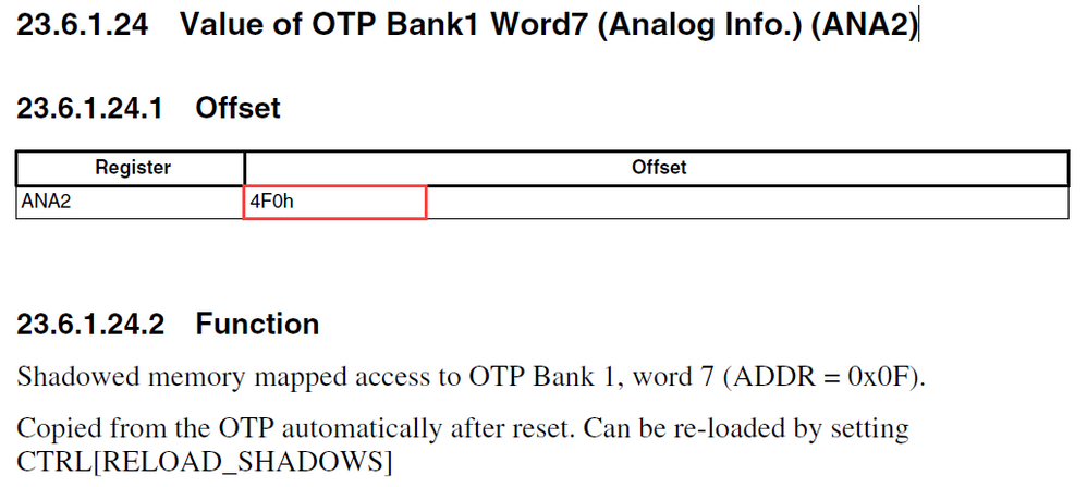
In section 23.6.1.24.2 of the reference manual, you will find the shadow register that corresponds to this word.
Here, you can see that the offset of this register is 4F0. If you go to the Fusemap Descriptions Table, you will see that address 0x4F0 corresponds to the USB VID and USB PID.
Have a great day,
Victor
-------------------------------------------------------------------------------
Note:
- If this post answers your question, please click the "Mark Correct"button. Thank you!
- We are following threads for 7 weeks after the last post, later replies are ignored
Please open a new thread and refer to the closed one, if you have a related question at a later point in time.
-------------------------------------------------------------------------------
Thanks for this post, now I gained access to CFG0(ADDR - 0x410) & CFG1(ADDR - 0x420) in fuse map for RT1064, the datasheet (Table22-6) says they are SJC CHALLENGE/Unique ID, I just wonder whether they are really unique, can be used as a unit specific unique ID.
Regards!
Ping
Hello Ed,
There is some misunderstanding regarding the capabilities of the shadow registers. Writing to the shadow registers doesn't affect at any level the corresponding fuses.
All fuse words in efusebox are shadowed. Therefore, fuse information is available through memory-mapped shadow registers. If fuses are subsequently programmed, the shadow registers should be reloaded to keep them coherent with the fuse bank arrays.
Shadow register bits can be overridden by software until the corresponding fuse lock bit for the region is set. When the lock shadow bit is set, the shadow registers for that lock region become write-locked.
The shadow registers automatically load the appropriate OTP contents after reset is deasserted. This means that once the power-up sequence is completed the fuse values will be copied directly into their corresponding shadowed registers. This is with the intended that you can read the fuse values in run-time.
To learn more information about how to read/write the shadow registers refer to sections 23.4.1.1, 23.4.1.2, and 23.4.1.3 of the reference manual.
Have a great day,
Victor
-------------------------------------------------------------------------------
Note:
- If this post answers your question, please click the "Mark Correct"button. Thank you!
- We are following threads for 7 weeks after the last post, later replies are ignored
Please open a new thread and refer to the closed one, if you have a related question at a later point in time.
-------------------------------------------------------------------------------
Hi Victor,
Thanks for responding, but that doesn't answer my question. I read the chapters, and I do realize that modifying the shadow registers does not affect the fusemap; but that's the extent of my understanding. The operations described in section 23.4.1 outline the steps to access the fusemap directly, I get that, here is my fundamental problem...
There appears to be two different sets of addresses for the fusemap...
Chapter 22 goes into good detail regarding addresses (and bit definitions) that range from 0x400-0x8c0, but then chapter 23 refers to the "Fuse Shadow Memory Footprint" which has addresses from 0x00-0x3f (and it gives zero information regarding bit descriptions).
Is the "ADDR" value (i.e. HW_OCOTP_CTRL[ADDR]) described in the sections you mention, the address documented in the "Fusemap Description Table" (chap22) or the "Fuse Shadow Memory Footprint" (chap23)?
Ed
Hi Ed,
I think I understood your confusion. For the explanation, I will take as an example the ANALOG group that is at location 0x0F.
In section 23.6.1.24.2 of the reference manual, you will find the shadow register that corresponds to this word.
Here, you can see that the offset of this register is 4F0. If you go to the Fusemap Descriptions Table, you will see that address 0x4F0 corresponds to the USB VID and USB PID.
Have a great day,
Victor
-------------------------------------------------------------------------------
Note:
- If this post answers your question, please click the "Mark Correct"button. Thank you!
- We are following threads for 7 weeks after the last post, later replies are ignored
Please open a new thread and refer to the closed one, if you have a related question at a later point in time.
-------------------------------------------------------------------------------
Hey Victor,
First of all sorry for the late reply. For some reason I don't get email anymore when a forum notification comes in for me... Not sure what broke there...
Anyway, I believe this solves my confusion, but just to be sure...
I see the correlation between 0x4F0 and Bank1 Word7 (referring to table 23.6.1.1); so am I correct to assume that I would use 0x0F (offset from Figure 23-2) as the address passed to OCOTP_ReadFuseShadowRegister() to read what is at 0x4F0 in the fusemap?
If that's the case, then you nailed it for me, and I'll mark this answered.
Thanks!
Ed
Hi Ed,
Yes, your understanding is correct. You need to pass 0x0F as the address argument to the function OCOTP_ReadFuseShadowRegister() to read what is at 0x4F0 in the fusemap.
Have a great day,
Victor
-------------------------------------------------------------------------------
Note:
- If this post answers your question, please click the "Mark Correct"button. Thank you!
- We are following threads for 7 weeks after the last post, later replies are ignored
Please open a new thread and refer to the closed one, if you have a related question at a later point in time.
-------------------------------------------------------------------------------
As an add-on to my above question, I see that MIMXRT1062.h has comments that seem to correlate various offsets into the OCOTP register space to addresses in the fusemap. For example, if I wanted to see the Default FlexRAM bank partitioning as defined by the fusemap, then I could read OCOTP->MISC_CONF0 and decode bits [19:16].
When I go to the reference manual and look at the description of the MISC_CONF0 I see this description...
and that seems to be the extent of the "Diagram" for most of these registers. So am I really supposed to refer to MIMXRT1062.h for the OCOTP documentation?
Hi Ed
This thread may give some extra details about matching up the eFUSE (and bit) settings with shadow registers:
https://community.nxp.com/message/1312044#comment-1312136
Regards
Mark
[uTasker project developer for Kinetis and i.MX RT]
Thanks Mark,
Still not clear to me, but it'll sink in sooner or later. I just don't understand why there are two different "address spaces" for the fuse maps. The reference manual goes into great detail on the 0x600-0x8c0 space, but then (as best I can tell) the NXP SDK uses the 0x00-0x3f addresses, but nowhere is there a mapping between the two different spaces. I saw your drawing, but it looks like that is in the GUI. I am more interested in a mapping explanation in the reference manual because I'm trying to avoid using the GUI.
Tx
Ed


