- Forums
- Product Forums
- General Purpose MicrocontrollersGeneral Purpose Microcontrollers
- i.MX Forumsi.MX Forums
- QorIQ Processing PlatformsQorIQ Processing Platforms
- Identification and SecurityIdentification and Security
- Power ManagementPower Management
- Wireless ConnectivityWireless Connectivity
- RFID / NFCRFID / NFC
- Advanced AnalogAdvanced Analog
- MCX Microcontrollers
- S32G
- S32K
- S32V
- MPC5xxx
- Other NXP Products
- S12 / MagniV Microcontrollers
- Powertrain and Electrification Analog Drivers
- Sensors
- Vybrid Processors
- Digital Signal Controllers
- 8-bit Microcontrollers
- ColdFire/68K Microcontrollers and Processors
- PowerQUICC Processors
- OSBDM and TBDML
- S32M
- S32Z/E
-
- Solution Forums
- Software Forums
- MCUXpresso Software and ToolsMCUXpresso Software and Tools
- CodeWarriorCodeWarrior
- MQX Software SolutionsMQX Software Solutions
- Model-Based Design Toolbox (MBDT)Model-Based Design Toolbox (MBDT)
- FreeMASTER
- eIQ Machine Learning Software
- Embedded Software and Tools Clinic
- S32 SDK
- S32 Design Studio
- GUI Guider
- Zephyr Project
- Voice Technology
- Application Software Packs
- Secure Provisioning SDK (SPSDK)
- Processor Expert Software
- Generative AI & LLMs
-
- Topics
- Mobile Robotics - Drones and RoversMobile Robotics - Drones and Rovers
- NXP Training ContentNXP Training Content
- University ProgramsUniversity Programs
- Rapid IoT
- NXP Designs
- SafeAssure-Community
- OSS Security & Maintenance
- Using Our Community
-
- Cloud Lab Forums
-
- Knowledge Bases
- ARM Microcontrollers
- i.MX Processors
- Identification and Security
- Model-Based Design Toolbox (MBDT)
- QorIQ Processing Platforms
- S32 Automotive Processing Platform
- Wireless Connectivity
- CodeWarrior
- MCUXpresso Suite of Software and Tools
- MQX Software Solutions
- RFID / NFC
- Advanced Analog
-
- NXP Tech Blogs
IMX8M PLUS || PCIe Interface || Clock Type
Hello NXP Team,
I want to know the information regarding the PCIe clock of IMX8M PLUS processor.
The PCIe Switch having which type of reference clock source.
Hi,
Thank you for your interest in NXP Semiconductor products,
This is the frequency requirement,
The requirements are complient with the PCI specification as mentioned in the datasheet but you can have a reference is the design and device of 8M Plus' PCI reference clock generator.
Regards
Hello @JosephAtNXP
Could you please brief about the purposes of using external PCIe clock generator used in the EVK board.
In our design we are planning to avoid external clock generator(9FGV0241AKLF) due to BOM optimization. So IMX 8M plus will act as a root complex device. So what will be the clock type from NXP processor?
and can we meet the standard PCIe clock requirement for the PCIe gen3.0 x1 Lane interface without using the external PCIe clock generator?
Hi,
This piece of information is from 8M Plus' reference manual:
The PLL in the CMN synthesizes high-speed clock, which is used for TX serializer and RX CDR lock, from a reference clock. The reference clock can be selected from two clock sources; internal SoC reference clock and external differential reference clock.
In the PCIe PHY, the high frequency clock from PLL is used in the serialization of TX data and CDR lock acquisition and maintenance.
You can optimize BOM and use the internal oscillator, the main reason to use an external oscillator is to have the same reference for both PCI EP and RC's CDR. So, it can be traded off.
Regards,
Hi @JosephAtNXP ,
Termination/differential signal standard used in MIMX8ML6CVNKZAB
We are interfacing NXP with a PCIe switch(PI7C9X3G606GPBFCA) without using external clock generator.
So, what will be the differential signal standard? is it HCSL?
And is it required to provide any kind of termination at driver side(NXP)?
Can we get some reference document to know the differential clock type used?
For providing the termination at endpoint(PCIe Switch) we need to know the more information about the differential clock type available at the source(NXP i.MX 8M Plus) side. Please guide to us.
Hi,
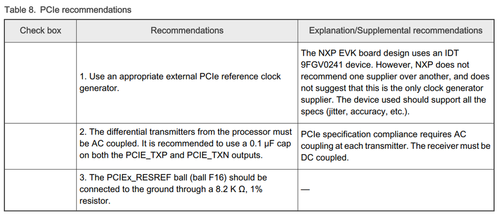
Here are the guidelines provided by the hardware developers guide:
And this is a backup found in hardware developers guide:
On EVK, a PCIE clock generator chip (9FGV0241) is used to feed high-quality clock to both the PHY and connecter/device. If a PCIE clock generator is not available, use the internal clock of the chip. Note that the internal clock exhibits larger jitter than that from PCIE clock generator
These are guidelines from a PCIe training:
Layout and Routing Guidelines based on 8Gbps rules:
− AC coupling caps placed symmetrically? Near one end of the
channel?
− AC coupling caps located near TX end when connector is
implemented in system
− TX and RX data and REFCLKs routed as diff pairs
− Diff pairs routed symmetrically?
− No stubs anywhere in the diff pair routing
− No routing over plane splits or anti-pads
− Oblique routing used for diff pairs
− Diff pair (P-N) matching to within 10 mils for TX and RX data diff
pairs
− Diff pair (P-N) matching to within 5 mil for REFCLK diff pairs
− Max length of all diff pairs on add-in card < 4 inches
− Diff pair length matching near the location of mismatch; within
guidelines for sectional jogs?
− Lane-to-lane skew within tolerance
− Serpentine bends within guideline (no sharp angles)
Regards,
Hi @JosephAtNXP
Attaching our use case. 
1) So which PCIe clock method is suggesting for us based on our use case? 
2) Which termination is suggesting for the PCIe clock?
Our concern about the clock is if we proceed with the method 2, then need to know about the clock type...then only we can provide corresponding clock termination/transformations. Refer the attached application note for this query.
Hi,
As said, you can use internal clock or external clock in any application just considering that there may be a larger jitter, this increment can be in any application, and as you may see in schematics, there are no clock termination requirement, check that if internal clock'd be used, map M2 pins to processor pins.
Regards,


