- Forums
- Product Forums
- General Purpose MicrocontrollersGeneral Purpose Microcontrollers
- i.MX Forumsi.MX Forums
- QorIQ Processing PlatformsQorIQ Processing Platforms
- Identification and SecurityIdentification and Security
- Power ManagementPower Management
- Wireless ConnectivityWireless Connectivity
- RFID / NFCRFID / NFC
- Advanced AnalogAdvanced Analog
- MCX Microcontrollers
- S32G
- S32K
- S32V
- MPC5xxx
- Other NXP Products
- S12 / MagniV Microcontrollers
- Powertrain and Electrification Analog Drivers
- Sensors
- Vybrid Processors
- Digital Signal Controllers
- 8-bit Microcontrollers
- ColdFire/68K Microcontrollers and Processors
- PowerQUICC Processors
- OSBDM and TBDML
- S32M
- S32Z/E
-
- Solution Forums
- Software Forums
- MCUXpresso Software and ToolsMCUXpresso Software and Tools
- CodeWarriorCodeWarrior
- MQX Software SolutionsMQX Software Solutions
- Model-Based Design Toolbox (MBDT)Model-Based Design Toolbox (MBDT)
- FreeMASTER
- eIQ Machine Learning Software
- Embedded Software and Tools Clinic
- S32 SDK
- S32 Design Studio
- GUI Guider
- Zephyr Project
- Voice Technology
- Application Software Packs
- Secure Provisioning SDK (SPSDK)
- Processor Expert Software
- Generative AI & LLMs
-
- Topics
- Mobile Robotics - Drones and RoversMobile Robotics - Drones and Rovers
- NXP Training ContentNXP Training Content
- University ProgramsUniversity Programs
- Rapid IoT
- NXP Designs
- SafeAssure-Community
- OSS Security & Maintenance
- Using Our Community
-
- Cloud Lab Forums
-
- Knowledge Bases
- ARM Microcontrollers
- i.MX Processors
- Identification and Security
- Model-Based Design Toolbox (MBDT)
- QorIQ Processing Platforms
- S32 Automotive Processing Platform
- Wireless Connectivity
- CodeWarrior
- MCUXpresso Suite of Software and Tools
- MQX Software Solutions
- RFID / NFC
- Advanced Analog
-
- NXP Tech Blogs
- Home
- :
- 製品フォーラム
- :
- S12 / MagniVマイクロコントローラ
- :
- Re: How to configure register of CPMU for external crystal?
How to configure register of CPMU for external crystal?
- RSS フィードを購読する
- トピックを新着としてマーク
- トピックを既読としてマーク
- このトピックを現在のユーザーにフロートします
- ブックマーク
- 購読
- ミュート
- 印刷用ページ
- 新着としてマーク
- ブックマーク
- 購読
- ミュート
- RSS フィードを購読する
- ハイライト
- 印刷
- 不適切なコンテンツを報告
Hi,
I have the code as attachment. It work fine (ADC & SCI using internal RC-Oscillator in S12ZVCA).
I want to add function of CAN-bus 250kbps. So, I add 12MHz external crystal in my board in order to have a good reliability for CAN.
.
How to setup the register of CPMU?
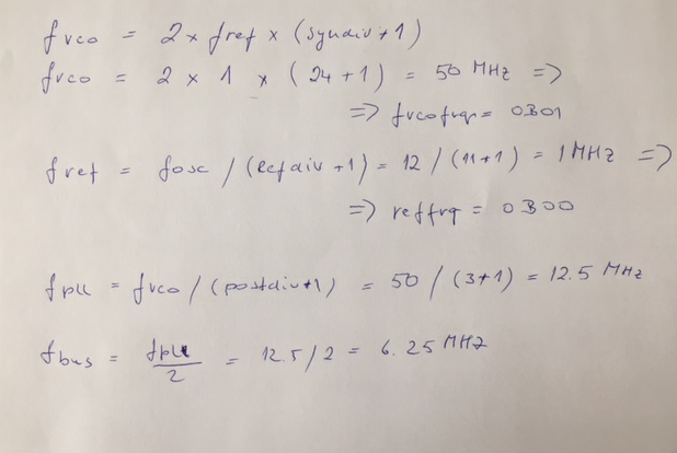
// fref = 1MHz, fVCO = 50MHz, fPLL = 12.5MHz
CPMUREFDIV = 0x0B; // fref = fosc/(refdiv+1) = 12 / (11 + 1) = 1MHz 00_00_1011
CPMUSYNR = 0x58; // fVCO = 2 * fref * (SYNDIV + 1) = 2 * (24+1) = 50MHz 01_011000
CPMUPOSTDIV = 0x03; //fPLL = fVCO / (POSTDIV + 1) = 50 / 4 = 12.5MHz 000_00011
fref = 1MHz, fVCO = 50MHz, fPLL = 12.5MHz can work on CAN-bus 250Kbps or not?
Can you give me some advice?
Best Regards,
Aaron
Original Attachment has been moved to: B0004-TestADC_ADC_UART_1.916Hz.rar
解決済! 解決策の投稿を見る。
- 新着としてマーク
- ブックマーク
- 購読
- ミュート
- RSS フィードを購読する
- ハイライト
- 印刷
- 不適切なコンテンツを報告
I am sorry I am not able to answer. I am not sure I have missed something but we have to think about different clocks:
1) BUSCLK frequency of the bus.
What value of BUSCLK you want to have?
2) OSCCLK frequency of the oscillator from which the busclk is derived. (12MHz in your case)
3) CANCLK - frequency of input clocks to a CAN module. The CANCLK can be OSCCLK or BUSCLK.
If the CANCLK is derived directly from OSCCLK the busclk does not influence CANCLK.
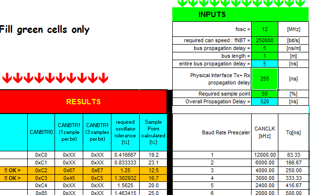
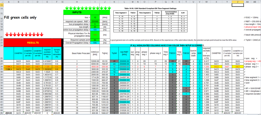
The results are highlighted. The only problem I see sample point. If it suits to you then it is OK.
I can see you use ATD and SCI in your example without any info about busclk from which the clock for these peripherals are derived. I have look at your SCI setup and you really use 6.25MHz busclk.
Now there are two ways:
1) Either select new busclk and adjust clock setup for SCI and ATD
2) or to use original clock setup for ATD and SCI peripherals and try to trim busclk to 6.25MHz.
If I assume item 2, then your original setup is OK and I suppose you do not want to change anything in the ATD and SCI peripheral setup, so:
| OSC[MHz] | SYNDIV | VCOFRQ | REFDIV | REFFRQ | POSTDIV | fref | fvco | fPLL | fvco/fref | fbus |
| 12 | 24 | 1 | 11 | 0 | 3 | 1 | 50 | 12.5 | 50 | 6.25 |
// make 6.25MHz BUSCLK from the external oscillator 12MHz
void CPMU_Init( void )
{
//============================================================================
ECLKCTL_NECLK = 0; //enable ECLK (BUSCLK at PP0)
//============================================================================
//Default state after reset:
// So after reset:
// CPMUOSC_OSCE == 0 => fref = firc1m = 1MHz
// CMPU_PLLSEL == 1 => fpll = fref / 4 = while not locked
// = 1MHz / 4 = 250kHz
// then fpll = 2 * fref *(syndiv+1) / (postdiv + 1) =
// = 2 * 1MHz *(24 +1) / (3 + 1) =
// = 50 / 4 = 12.5MHz
// fbus = fpll / 6.25MHz
Delay( 1000 ); //delay in order to see default bus frequency on ECLK output
//============================================================================
// PLL setup 16 MHz BUSCLK from 4 MHz
// expected frequency after lose of OSC, PEE, PBE:
// - fbus= fpll/2= 1/4MHz/2 = 125 kHz till locked then
// - fbus= fpll/2= 2*fref*(syndiv+1)/(postdiv + 1)/2 = 2*1*25/(3+1)/2=6.25MHz
CPMUSYNR = 0x58; // 0B01_0x18
CPMUREFDIV = 0x0B; // 0B00_0x0B
CPMUPOSTDIV = 0x03;
CPMUOSC_OSCE = 1;
while( CPMUIFLG_UPOSC == 0 )
{
__RESET_WATCHDOG(); // if COP is enabled by HW then it should be served in loops
// add some code for time out error
}
// PLLSEL - CPMUCLKS_PLLSEL = 1; // PEE ; CPMUCLKS_PLLSEL = 0; // PBE
// PSTP - COP stopped in STOP mode
// CSAD - COP stopped in STOP mode
// COPOSCSEL1 = 0; COP clock derived by COPOSCSEL0
// PRE - RTI disabled when pseudo STOP
// PCE - COP stopped in pseudo STOP mode
// RTIOSCSEL - RTI clock source is IRCCLK
// COPOSCSEL0 = 0; COP clock source IRCCLK
// After writing CPMUCLKS register, it is strongly recommended to read
// back CPMUCLKS register to make sure that write of PLLSEL,
// RTIOSCSEL and COPOSCSEL was successful. This is because under
// certain circumstances writes have no effect or bits are automatically
// changed
// You can add some timeout into the loop if required
do
{
//CPMUCLKS = 0B10100000;
CPMUCLKS = 0B10000000;
// add some code for time out error
}
// while( CPMUCLKS != 0B10100000);
while( CPMUCLKS != 0B10000000);
#ifdef COP_EXAMPLE
CPMUCOP = 0B01000101; //4.194304s till timeout, 1MHz IRCCLK used by default
//RSBCK == 1; COP and RTI Stop in Active BDM Mode Bit
#endif
// voltage regulator selections
// select power option
//.........................................
//Note: Write once Register
//CPMUVREGCTL = 0x06; //Turn on Ballast transistor for VDDX domain
//and switch on regulator for VDDC domain
//OR
CPMUVREGCTL = 0x05; //Internal voltage regulator for VDDX domain
//and switch on regulator for VDDC domain
}
Best regards,
Ladislav
- 新着としてマーク
- ブックマーク
- 購読
- ミュート
- RSS フィードを購読する
- ハイライト
- 印刷
- 不適切なコンテンツを報告
Hi,
I see no problem with the current setup. Everything is working correctly. If there are no special expectations for calculations or processing tasks then current setup is OK.
The only thing I HAVE TO correct is the excel sheet I sent to you. There is a mistake in the sample point calculation. I have corrected it in this version CAN_setup6.zip.
best regards,
Ladislav
- 新着としてマーク
- ブックマーク
- 購読
- ミュート
- RSS フィードを購読する
- ハイライト
- 印刷
- 不適切なコンテンツを報告
Hi Ladislav,
Your code of CPMU_Init() (as following) can work fine for ADC & SCI. Thank you.
I wrote CAN_Init() & CANPHY_Init() as following. Do you have any recommendations ?
void CAN_init(void)
{
// initialise MSCAN
CAN0CTL0 = 0x01; // MSCAN in initialization mode
while (!(CAN0CTL1_INITAK)){} // Loop when Initialization mode inactive
CAN0CTL1_CANE = 1; // Enable MSCAN module
CAN0CTL1_CLKSRC = 0; // Clock source is OSCCLK = 12 MHz
CAN0CTL1_LOOPB = 0; // DISABLE LoopBack Mode
CAN0CTL1_LISTEN = 0; // Not listen only mode
CAN0CTL0_WUPE = 1; // Enable WAKEUP//Baud rate = CANCLK/(Pre-scaler * time quanta)
CAN0BTR0 = 0xC2; // SJW = 3 (4 Tq clock cycles), BRP = 2 (Baud Rate Prescaler = 3, CANCLK = 12MHz/3=4MHz)
CAN0BTR1 = 0xE7; // 3 Sample/bit, TSEG2=6 (Time Segment 2 = 7 Tq clock cycles), TSEG1=7 (Time Segment 1 = 8 Tq clock cycles)//accept all messages
CAN0IDAC_IDAM = 0; /* Two 32 bit filters */
CAN0IDMR0 = 0xFF; /* Accept all incoming ID's */
CAN0IDMR1 = 0xFF;
CAN0IDMR2 = 0xFF;
CAN0IDMR3 = 0xFF;
CAN0IDMR4 = 0xFF;
CAN0IDMR5 = 0xFF;
CAN0IDMR6 = 0xFF;
CAN0IDMR7 = 0xFF;
//exit initialization mode
CAN0CTL0_INITRQ = 0;
while (CAN0CTL1_INITAK){};
while(!(CAN0CTL0_SYNCH)){};
//clear flags
CAN0RFLG_RXF = 1;
CAN0RIER_RXFIE = 1;
}void CANPHY_init(void)
{
//enable physical layer
CP0CR_CPE = 1; // ENABLE CAN Physical
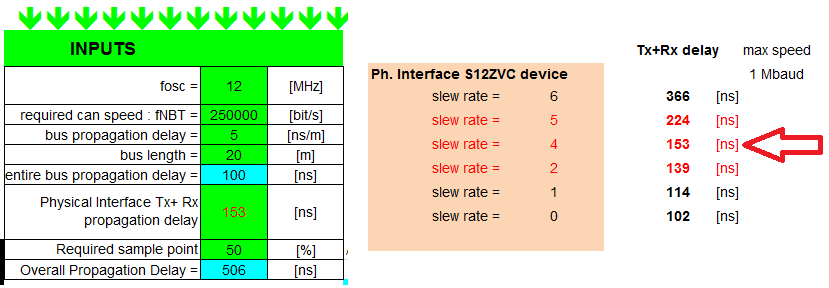
CP0CR_SLR = 4; // Slew Rate = 4 (Tx+Rx delay = 153ns)
CP0IE = 0; // DISABLE Interrupts
CP0CR_SPE = 1; // ENABLE SPLIT = 2.5V
CP0CR_WUPEI = 1; // Configure Wake-up (01: ENABLE wake-up receiver, 1st wake-up event is masked)
}
Best Regards,
Aaron
- 新着としてマーク
- ブックマーク
- 購読
- ミュート
- RSS フィードを購読する
- ハイライト
- 印刷
- 不適切なコンテンツを報告
Hi,
If you decided to use 60% from other results then OK.
Only comment: A good general rule is to set the sample point above 80%. Based on the experiences of the automotive industry, the selected sample point should be near the 80% value.
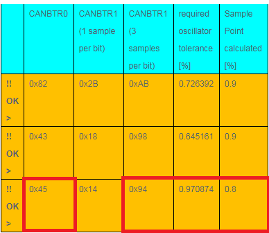
| CANBTR0 | CANBTR1 (1 sample per bit) | CANBTR1 (3 samples per bit) | required oscillator tolerance [%] | Sample Point |
!! OK > | 0x82 | 0x2B | 0xAB | 0.726392 | 0.9 |
!! OK > | 0x43 | 0x18 | 0x98 | 0.645161 | 0.9 |
!! OK > | 0x45 | 0x14 | 0x94 | 0.970874 | 0.8 |
The setup:
1)
while (CAN0CTL1_INITAK){};
while(!(CAN0CTL0_SYNCH)){};
I would suggest you to add to these loops some counter (incrementing/decrementing variable) which will counts the most acceptable time to avoid never-ending loop. If counter overflows/reaches zero then you should try again or report error to the system.
2)
Incorrect flags clearing approach. Probably in this case will not cause any error but in another case it can cause big issues.
WRONG:
//clear flags
CAN0RFLG_RXF = 1; // clears all flags because instruction is internally performed as read-modify-write
CAN0RIER_RXFIE = 1;
Correct:
CAN0RFLG = 0x01; // clears RxF only, all other flags will remain unchanged
Please refer to an application note: http://www.nxp.com/docs/en/application-note/AN2617.pdf
Best regards,
Ladislav
- 新着としてマーク
- ブックマーク
- 購読
- ミュート
- RSS フィードを購読する
- ハイライト
- 印刷
- 不適切なコンテンツを報告
Hi Ladislav,
I only see 2 rows show "OK". What's wrong?
I will modify my code by following your reply later. Thank you.
Best Regards,
Aaron
- 新着としてマーク
- ブックマーク
- 購読
- ミュート
- RSS フィードを購読する
- ハイライト
- 印刷
- 不適切なコンテンツを報告
Hi,
change sample point (input parameter) in the cell $I$22 to 80% and results will change.
best regards,
Ladislav
- 新着としてマーク
- ブックマーク
- 購読
- ミュート
- RSS フィードを購読する
- ハイライト
- 印刷
- 不適切なコンテンツを報告
- 新着としてマーク
- ブックマーク
- 購読
- ミュート
- RSS フィードを購読する
- ハイライト
- 印刷
- 不適切なコンテンツを報告
Hi Ladislav,
I resolved the issue.
Wrong:
MODRR0 = 0x26;
Correct:
MODRR0 = 0x24;
Any recommend about my code?
Best Regard,
Aaron
- 新着としてマーク
- ブックマーク
- 購読
- ミュート
- RSS フィードを購読する
- ハイライト
- 印刷
- 不適切なコンテンツを報告
Hi,
I am sorry I am taking vacation. I'll look at it next week if still necessary.
Best regards,
Ladislav
- 新着としてマーク
- ブックマーク
- 購読
- ミュート
- RSS フィードを購読する
- ハイライト
- 印刷
- 不適切なコンテンツを報告
Hi,
the best clock and clock stability you get if you do not supply clock from PLL but directly from the oscillator.
in this case you should select proper oscillator frequency for CAN bit timing and then set CLKSRC bit in the CANCTL1 to 0.
register CANCTL1:
bit CLKSRC: MSCAN Clock Source — This bit defines the clock source for the MSCAN module (only for systems with a clock
generation module; Section 18.4.3.2, “Clock System,” and Section Figure 18-43., “MSCAN Clocking Scheme,”).
0 MSCAN clock source is the oscillator clock
1 MSCAN clock source is the bus clock
However, if you are still decided to use fbus as a source clock for can then I would like to be sure you want to use
fbus = 6.25MHz because you set fpll to 12.5MHz in your setup. If there is anything wrong then I would like to ask you to provide busclk=fbus you want to set.
Finally, when I have your inputs, I will send you and code example.
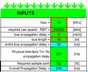
For CAN setup you can use attached excel sheet.
Best regards,
Ladislav
- 新着としてマーク
- ブックマーク
- 購読
- ミュート
- RSS フィードを購読する
- ハイライト
- 印刷
- 不適切なコンテンツを報告
Hi Ladislav,
I only know the parameter of marked (12, 250000 & 10).
I want to use CLKSRC=0 (MSCAN clock source is the oscillator clock) & internal physical interface in S12ZVC.
Best Regards,
Aaron
- 新着としてマーク
- ブックマーク
- 購読
- ミュート
- RSS フィードを購読する
- ハイライト
- 印刷
- 不適切なコンテンツを報告
I am sorry I am not able to answer. I am not sure I have missed something but we have to think about different clocks:
1) BUSCLK frequency of the bus.
What value of BUSCLK you want to have?
2) OSCCLK frequency of the oscillator from which the busclk is derived. (12MHz in your case)
3) CANCLK - frequency of input clocks to a CAN module. The CANCLK can be OSCCLK or BUSCLK.
If the CANCLK is derived directly from OSCCLK the busclk does not influence CANCLK.
The results are highlighted. The only problem I see sample point. If it suits to you then it is OK.
I can see you use ATD and SCI in your example without any info about busclk from which the clock for these peripherals are derived. I have look at your SCI setup and you really use 6.25MHz busclk.
Now there are two ways:
1) Either select new busclk and adjust clock setup for SCI and ATD
2) or to use original clock setup for ATD and SCI peripherals and try to trim busclk to 6.25MHz.
If I assume item 2, then your original setup is OK and I suppose you do not want to change anything in the ATD and SCI peripheral setup, so:
| OSC[MHz] | SYNDIV | VCOFRQ | REFDIV | REFFRQ | POSTDIV | fref | fvco | fPLL | fvco/fref | fbus |
| 12 | 24 | 1 | 11 | 0 | 3 | 1 | 50 | 12.5 | 50 | 6.25 |
// make 6.25MHz BUSCLK from the external oscillator 12MHz
void CPMU_Init( void )
{
//============================================================================
ECLKCTL_NECLK = 0; //enable ECLK (BUSCLK at PP0)
//============================================================================
//Default state after reset:
// So after reset:
// CPMUOSC_OSCE == 0 => fref = firc1m = 1MHz
// CMPU_PLLSEL == 1 => fpll = fref / 4 = while not locked
// = 1MHz / 4 = 250kHz
// then fpll = 2 * fref *(syndiv+1) / (postdiv + 1) =
// = 2 * 1MHz *(24 +1) / (3 + 1) =
// = 50 / 4 = 12.5MHz
// fbus = fpll / 6.25MHz
Delay( 1000 ); //delay in order to see default bus frequency on ECLK output
//============================================================================
// PLL setup 16 MHz BUSCLK from 4 MHz
// expected frequency after lose of OSC, PEE, PBE:
// - fbus= fpll/2= 1/4MHz/2 = 125 kHz till locked then
// - fbus= fpll/2= 2*fref*(syndiv+1)/(postdiv + 1)/2 = 2*1*25/(3+1)/2=6.25MHz
CPMUSYNR = 0x58; // 0B01_0x18
CPMUREFDIV = 0x0B; // 0B00_0x0B
CPMUPOSTDIV = 0x03;
CPMUOSC_OSCE = 1;
while( CPMUIFLG_UPOSC == 0 )
{
__RESET_WATCHDOG(); // if COP is enabled by HW then it should be served in loops
// add some code for time out error
}
// PLLSEL - CPMUCLKS_PLLSEL = 1; // PEE ; CPMUCLKS_PLLSEL = 0; // PBE
// PSTP - COP stopped in STOP mode
// CSAD - COP stopped in STOP mode
// COPOSCSEL1 = 0; COP clock derived by COPOSCSEL0
// PRE - RTI disabled when pseudo STOP
// PCE - COP stopped in pseudo STOP mode
// RTIOSCSEL - RTI clock source is IRCCLK
// COPOSCSEL0 = 0; COP clock source IRCCLK
// After writing CPMUCLKS register, it is strongly recommended to read
// back CPMUCLKS register to make sure that write of PLLSEL,
// RTIOSCSEL and COPOSCSEL was successful. This is because under
// certain circumstances writes have no effect or bits are automatically
// changed
// You can add some timeout into the loop if required
do
{
//CPMUCLKS = 0B10100000;
CPMUCLKS = 0B10000000;
// add some code for time out error
}
// while( CPMUCLKS != 0B10100000);
while( CPMUCLKS != 0B10000000);
#ifdef COP_EXAMPLE
CPMUCOP = 0B01000101; //4.194304s till timeout, 1MHz IRCCLK used by default
//RSBCK == 1; COP and RTI Stop in Active BDM Mode Bit
#endif
// voltage regulator selections
// select power option
//.........................................
//Note: Write once Register
//CPMUVREGCTL = 0x06; //Turn on Ballast transistor for VDDX domain
//and switch on regulator for VDDC domain
//OR
CPMUVREGCTL = 0x05; //Internal voltage regulator for VDDX domain
//and switch on regulator for VDDC domain
}
Best regards,
Ladislav
- 新着としてマーク
- ブックマーク
- 購読
- ミュート
- RSS フィードを購読する
- ハイライト
- 印刷
- 不適切なコンテンツを報告
Hi Ladislav,
Actually, I don't know what value of BUSCLK is best.
In our case, the objectives were as follows:
- measure a analog signal and convert to digital value
- sent the digital value to UART(9600bps) or CAN-bus(250Kbps)
- sent 2~10 sample/second
What do you recommend?
