- Forums
- Product Forums
- General Purpose MicrocontrollersGeneral Purpose Microcontrollers
- i.MX Forumsi.MX Forums
- QorIQ Processing PlatformsQorIQ Processing Platforms
- Identification and SecurityIdentification and Security
- Power ManagementPower Management
- Wireless ConnectivityWireless Connectivity
- RFID / NFCRFID / NFC
- Advanced AnalogAdvanced Analog
- MCX Microcontrollers
- S32G
- S32K
- S32V
- MPC5xxx
- Other NXP Products
- S12 / MagniV Microcontrollers
- Powertrain and Electrification Analog Drivers
- Sensors
- Vybrid Processors
- Digital Signal Controllers
- 8-bit Microcontrollers
- ColdFire/68K Microcontrollers and Processors
- PowerQUICC Processors
- OSBDM and TBDML
- S32M
- S32Z/E
-
- Solution Forums
- Software Forums
- MCUXpresso Software and ToolsMCUXpresso Software and Tools
- CodeWarriorCodeWarrior
- MQX Software SolutionsMQX Software Solutions
- Model-Based Design Toolbox (MBDT)Model-Based Design Toolbox (MBDT)
- FreeMASTER
- eIQ Machine Learning Software
- Embedded Software and Tools Clinic
- S32 SDK
- S32 Design Studio
- GUI Guider
- Zephyr Project
- Voice Technology
- Application Software Packs
- Secure Provisioning SDK (SPSDK)
- Processor Expert Software
- Generative AI & LLMs
-
- Topics
- Mobile Robotics - Drones and RoversMobile Robotics - Drones and Rovers
- NXP Training ContentNXP Training Content
- University ProgramsUniversity Programs
- Rapid IoT
- NXP Designs
- SafeAssure-Community
- OSS Security & Maintenance
- Using Our Community
-
- Cloud Lab Forums
-
- Knowledge Bases
- ARM Microcontrollers
- i.MX Processors
- Identification and Security
- Model-Based Design Toolbox (MBDT)
- QorIQ Processing Platforms
- S32 Automotive Processing Platform
- Wireless Connectivity
- CodeWarrior
- MCUXpresso Suite of Software and Tools
- MQX Software Solutions
- RFID / NFC
- Advanced Analog
-
- NXP Tech Blogs
- Home
- :
- Product Forums
- :
- S12 / MagniV Microcontrollers
- :
- How to Current Measurement Calibrate
How to Current Measurement Calibrate
- Subscribe to RSS Feed
- Mark Topic as New
- Mark Topic as Read
- Float this Topic for Current User
- Bookmark
- Subscribe
- Mute
- Printer Friendly Page
How to Current Measurement Calibrate
- Mark as New
- Bookmark
- Subscribe
- Mute
- Subscribe to RSS Feed
- Permalink
- Report Inappropriate Content
How to calibrate current measurement in s12z microcontroller (I need to calibration procedure)Please help
- Mark as New
- Bookmark
- Subscribe
- Mute
- Subscribe to RSS Feed
- Permalink
- Report Inappropriate Content
Hi,
Could you elaborate on your request?
Which S12Z derivative do you use?
Regards,
Daniel
- Mark as New
- Bookmark
- Subscribe
- Mute
- Subscribe to RSS Feed
- Permalink
- Report Inappropriate Content
I am using mm9z1j638 need temperature and current calibration procedure for this controller
- Mark as New
- Bookmark
- Subscribe
- Mute
- Subscribe to RSS Feed
- Permalink
- Report Inappropriate Content
Hi,
the calibration is a quite complex process and the MM9Z1_638 device allows different options on how to use it, e.g. automatic temperature gain compensation or manual gain compensation using chip temperature result and lookup tables. Also the acquisition channel configuration used during operation has to be considered.
The system calibration should be performed as an incremental (incremental to NXP provided device calibration data) calibration.
The basic steps are:
- Characterize system behavior (applying device compensation values)
- Estimate deviation between real and ideal behavior (calculate delta between ideal behavior and measured behavior)
- Calculate incremental compensation values (delta values)
- Apply compensation during operation and verify system behavior
The following picture indicates which information / data is required to calculate the incremental gain and offset adjustments (gainsteps, offsetsteps).
For a good estimation of the acquisition channels behavior, e.g. a 5-point measurement is suitable.
The selection of the individual data points should consider application requirements like:
- desired input range
- area where highest accuracy is desired
- capability of the module / device (e.g. minimum supply voltage for Vsup)
- capability of equipment (e.g. max. Iout of power supplies, max. input range of DMM and related accuracy in the range)
- select current points for ISENSE calibration such that no gain switching is required
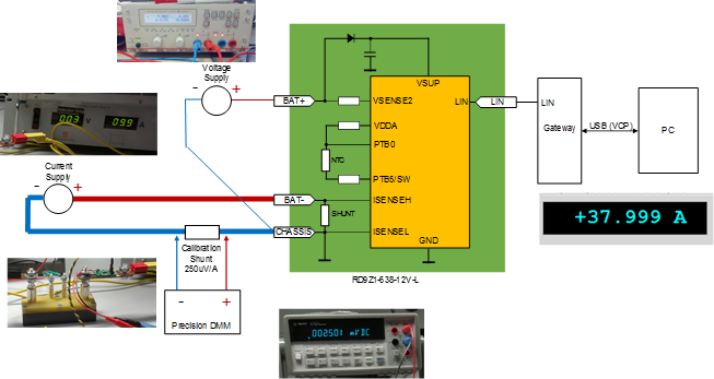
The picture below shows an example setup for the ISENSE channel compensation:
To discuss further details it might be better to directly discuss your applications needs?
Rgds
Wolfgang


