
- Forums
- Product Forums
- General Purpose MicrocontrollersGeneral Purpose Microcontrollers
- i.MX Forumsi.MX Forums
- QorIQ Processing PlatformsQorIQ Processing Platforms
- Identification and SecurityIdentification and Security
- Power ManagementPower Management
- Wireless ConnectivityWireless Connectivity
- RFID / NFCRFID / NFC
- Advanced AnalogAdvanced Analog
- Neural Processing UnitsNeural Processing Units
- MCX Microcontrollers
- S32G
- S32K
- S32V
- MPC5xxx
- Other NXP Products
- S12 / MagniV Microcontrollers
- Powertrain and Electrification Analog Drivers
- Sensors
- Vybrid Processors
- Digital Signal Controllers
- 8-bit Microcontrollers
- ColdFire/68K Microcontrollers and Processors
- PowerQUICC Processors
- OSBDM and TBDML
- S32M
- S32Z/E
-
- Solution Forums
- Software Forums
- MCUXpresso Software and ToolsMCUXpresso Software and Tools
- CodeWarriorCodeWarrior
- MQX Software SolutionsMQX Software Solutions
- Model-Based Design Toolbox (MBDT)Model-Based Design Toolbox (MBDT)
- FreeMASTER
- eIQ Machine Learning Software
- Embedded Software and Tools Clinic
- S32 SDK
- S32 Design Studio
- GUI Guider
- Zephyr Project
- Voice Technology
- Application Software Packs
- Secure Provisioning SDK (SPSDK)
- Processor Expert Software
- Generative AI & LLMs
-
- Topics
- Mobile Robotics - Drones and RoversMobile Robotics - Drones and Rovers
- NXP Training ContentNXP Training Content
- University ProgramsUniversity Programs
- Rapid IoT
- NXP Designs
- SafeAssure-Community
- OSS Security & Maintenance
- Using Our Community
-
- Cloud Lab Forums
-
- Knowledge Bases
- ARM Microcontrollers
- i.MX Processors
- Identification and Security
- Model-Based Design Toolbox (MBDT)
- QorIQ Processing Platforms
- S32 Automotive Processing Platform
- Wireless Connectivity
- CodeWarrior
- MCUXpresso Suite of Software and Tools
- MQX Software Solutions
- RFID / NFC
- Advanced Analog
- Neural Processing Units
-
- NXP Tech Blogs
- Home
- :
- QorIQプロセッシングプラットフォーム
- :
- QorIQ
- :
- Re: DDR Mapping Registers
DDR Mapping Registers
- RSS フィードを購読する
- トピックを新着としてマーク
- トピックを既読としてマーク
- このトピックを現在のユーザーにフロートします
- ブックマーク
- 購読
- ミュート
- 印刷用ページ

- 新着としてマーク
- ブックマーク
- 購読
- ミュート
- RSS フィードを購読する
- ハイライト
- 印刷
- 不適切なコンテンツを報告
Hi,
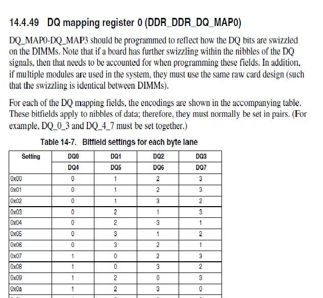
I am trying to configure the DDR Memory Controller's registers of T1042. I am done with many, but i am unable to comprehend the "DQ mapping registers." Can anybody explain what they are for and how to configure them?
Please find the attached image for your information. Thank you!
解決済! 解決策の投稿を見る。
 Bulat
Bulat
- 新着としてマーク
- ブックマーク
- 購読
- ミュート
- RSS フィードを購読する
- ハイライト
- 印刷
- 不適切なコンテンツを報告
Those registers are intended for future use with extended DDR4 features. At the moment (with current DDR4 controller) the user can leave default values.
Regards,
Bulat
 michelle
- 新着としてマーク
- ブックマーク
- 購読
- ミュート
- RSS フィードを購読する
- ハイライト
- 印刷
- 不適切なコンテンツを報告
Hi,
I am not sure where the previous poster found this as an unsupported feature for the DDR controller. DQ remappings are not normally included with uboot as our reference boards don't swizzle the data bus typically and we just take the HW defaults which are 1:1. However, we have seen this added to support bit ordering that isn't 0-31 sequentially on custom boards. The mappings are added in the board specific files along with the other DDR settings/configurations. For DDR validation you may need to modify some python scripts to make it work (to match your DQ swizzle).
The DQ mappings are as described... Each Nibble has 38h different orderings that can be used to move the bit order on any Nibble to accommodate bits 0-3 or 4-7 in different orders. This is available for all nibbles of the DDR bus and ECC lanes as well. This is in the hardware to specifically help support board layouts where a sequential order was difficult to achieve.
To get the correct mappings you would need to review and tabularize your DQ pin mappings to the DDR itself from your board's schematics and configure accordingly. The RM chapter 15.4.49 Contains all of the necessary details. A setting of 0x00 maps 1:1 bits 0-3 to bits 0-3, a setting of 0x18 for the nibble maps bits 0-3 to bits 3-0...
Hope this helps?
- 新着としてマーク
- ブックマーク
- 購読
- ミュート
- RSS フィードを購読する
- ハイライト
- 印刷
- 不適切なコンテンツを報告
Thank you for the info. I've read the refernced docs. Based on them it seems that the swizzling between nibbles is not allowed, so for example I can't swap the bit2 with the bit6 because they're in two separate nibbles. Is it so?
In the CodeWarrior validation tool I can't set swizzle option that swizzles between two nibbles.
And also if I make even one mapping register on a working configuration it makes it bad and the validation will not work anymore.
regards,
Gabor
Bulat
- 新着としてマーク
- ブックマーク
- 購読
- ミュート
- RSS フィードを購読する
- ハイライト
- 印刷
- 不適切なコンテンツを報告
Those registers are intended for future use with extended DDR4 features. At the moment (with current DDR4 controller) the user can leave default values.
Regards,
Bulat
- 新着としてマーク
- ブックマーク
- 購読
- ミュート
- RSS フィードを購読する
- ハイライト
- 印刷
- 不適切なコンテンツを報告
Hello,
I'm struggling with the DDR controller and I have this problem, too. I don't understand exactly what the defaults are for these reagisters. We have a working evalboard (LS1046ARDB) and if I set these registers to their defaults using QCVS Validation Tool the validation process will fail. If I create a QorIQ configuration project and read the memory settings from the evalboard's DIMM these values are set to a particular values and if I change just one the validation process will fail too.
We've made our custom board with 4GB of DDR4 and can't bring-up the memory controller. In the very first step of the validation process (Auto search & detect for write leveling start values ) after a while the process stops with message "The validation cannot proceed due to other hardware or software issues".
In our design we've made some "swizzling" inside the byte lanes, and also between the nibbles as well.
So, my question is what the correct DQ mapping values are.
Thanks in advance,
Gabor
