- Forums
- Product Forums
- General Purpose MicrocontrollersGeneral Purpose Microcontrollers
- i.MX Forumsi.MX Forums
- QorIQ Processing PlatformsQorIQ Processing Platforms
- Identification and SecurityIdentification and Security
- Power ManagementPower Management
- Wireless ConnectivityWireless Connectivity
- RFID / NFCRFID / NFC
- Advanced AnalogAdvanced Analog
- MCX Microcontrollers
- S32G
- S32K
- S32V
- MPC5xxx
- Other NXP Products
- S12 / MagniV Microcontrollers
- Powertrain and Electrification Analog Drivers
- Sensors
- Vybrid Processors
- Digital Signal Controllers
- 8-bit Microcontrollers
- ColdFire/68K Microcontrollers and Processors
- PowerQUICC Processors
- OSBDM and TBDML
- S32M
-
- Solution Forums
- Software Forums
- MCUXpresso Software and ToolsMCUXpresso Software and Tools
- CodeWarriorCodeWarrior
- MQX Software SolutionsMQX Software Solutions
- Model-Based Design Toolbox (MBDT)Model-Based Design Toolbox (MBDT)
- FreeMASTER
- eIQ Machine Learning Software
- Embedded Software and Tools Clinic
- S32 SDK
- S32 Design Studio
- GUI Guider
- Zephyr Project
- Voice Technology
- Application Software Packs
- Secure Provisioning SDK (SPSDK)
- Processor Expert Software
-
- Cloud Lab Forums
- Topics
- Mobile Robotics - Drones and RoversMobile Robotics - Drones and Rovers
- NXP Training ContentNXP Training Content
- University ProgramsUniversity Programs
- Rapid IoT
- NXP Designs
- SafeAssure-Community
- OSS Security & Maintenance
- Using Our Community
-
-
- Knowledge Bases
- ARM Microcontrollers
- Identification and Security
- i.MX Processors
- Model-Based Design Toolbox (MBDT)
- QorIQ Processing Platforms
- S32 Automotive Processing Platform
- CodeWarrior
- Wireless Connectivity
- MCUXpresso Suite of Software and Tools
- MQX Software Solutions
- RFID / NFC
- Advanced Analog
-
- Home
- :
- Software Forums
- :
- Processor Expert Software Knowledge Base
- :
- Low power demo application on FRDM-KL03Z board
Low power demo application on FRDM-KL03Z board
- Subscribe to RSS Feed
- Mark as New
- Mark as Read
- Bookmark
- Subscribe
- Printer Friendly Page
- Report Inappropriate Content
Low power demo application on FRDM-KL03Z board
Low power demo application on FRDM-KL03Z board
This document describes the creation of the following low power demo application:
When the application starts the green LED blink one time, The RTC device alarm is set to 15 second (external oscillator 32768Hz is used) to wakeup CPU and the CPU enters the VLLS1 mode (VLLS0 mode cannot be used with external oscillator).
The CPU wake up is possible by the following ways:
- When you push the SW2 button the processor is woken up and the green LED start blinking (5 times).
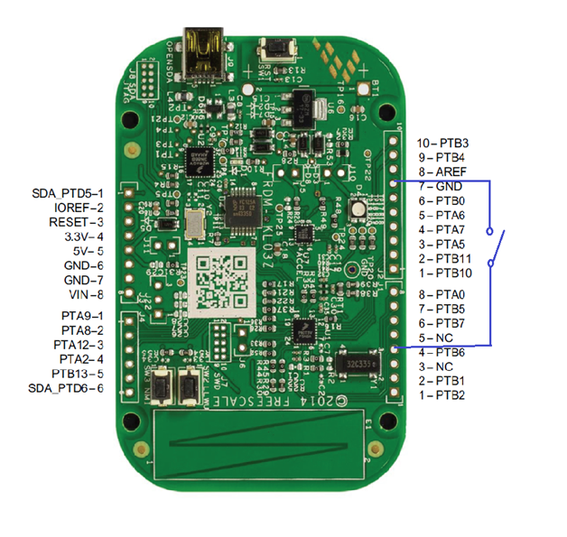
- When you short the pin PTB6 to ground 5 times (the pin is available on the 8 pin header connector – pin number 4; you can for example connect a button to the pin number 4 and ground) the processor is woken and the green LED start blinking (5 times).
- When selected RTC timeout expired (15 seconds) the processor is woken by the alarm interrupt and the green LED start blinking (5 times).
The application is initialized again and recovery from the VLLS1 mode is executed. The alarm is set to 15 second and the CPU enters the VLLS1 mode again.
Preparation
First of all the KDS 1.1.1 (KDS 2.0.0) and KSDK 1.0.0 for KL03Z must be installed. You can find instructions in the document How to install KL03 SDK support in KDS 1.1.1 and KDS 2.0.0.
New project
When you properly install and update all the software you are prepared to create the Low power demo application.
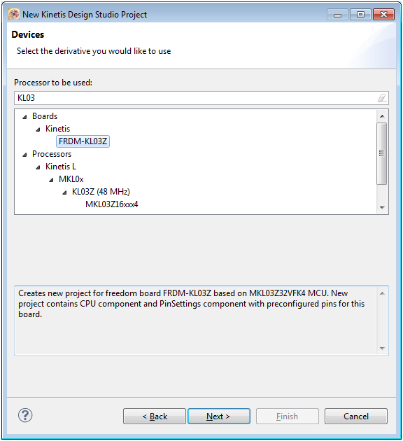
Create a new Kinetis design Studio project:
Select the FRDM-KL03Z board
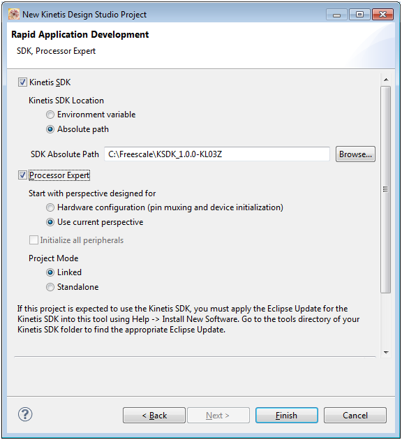
Select the Kinetis SDK path to the KSDK 1.0.0 for KL03Z and select Processor Expert
The application is created but there are many warnings reported in the Problems window saying that there is a conflict:
Ignored error: Selected value is in conflict with other configuration(s) property 'Pin 13', property 'CH1 - Channel 1', property 'Pin' from component gpio_pins, property 'ERCLK32K clock output' Exclusive connection required by property 'CH1 - Channel 1'; Selected value is in conflict with other configuration property 'CH1 - Channel 1', conflict in configuration of MUX bit-field of PORTB_PCR13 register. ; Selected value is in conflict with other configuration property 'Pin 13', property 'Pin' from component gpio_pins, conflict in configuration of MUX bit-field of PORTB_PCR13 register. (CLKOUT - Oscillator output), Low power demo KL03, ....
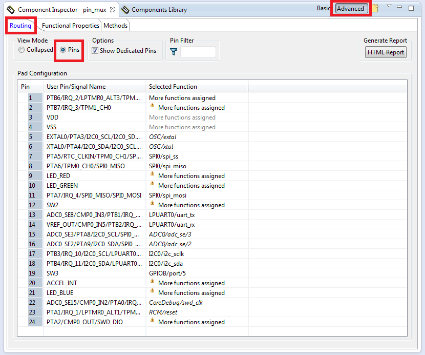
To resolve all these warnings you need to select the required functionality of reported pins in the PinSettings component: Open the Component Inspector of the PinSettings component, select the Routing tab and select the Pins View mode. All pins are available on one tab and you see small exclamation icons in rows where are reported conflicts:
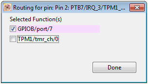
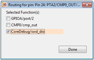
Click on each item with warning icon (the Selected Function row) and uncheck unused function of the pin to select one function only, i.e. you need to specify which functionality of the pin is initialized by code generated by Processor Expert.
You can select GPIO functionality in all case except the last pin number 24 that is used by debugger as swd_dio pin:
You can see that there is not any warning now and all pins are routed according to the selection you have done.
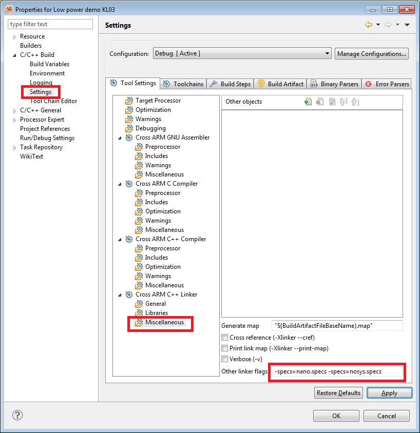
There is also necessary to change the linker settings when you have installed the new version of GCC tools (according to the document that is available in the KSDK 1.0.0 for KL03Z installation folder in KSDK_1.0.0-KL03Z\doc\Kinetis SDK Freescale Freedom FRDM-KL03Z Platform User’s Guide.pdf – chapter Appendix B: Kinetis Design Studio environment variable fix and swap tool chain)
Open the context menu of the project, select Properties item and change the Other linker flags settings to “-specs=nano.specs -specs=nosys.specs”, in C/C++ Build / Settings, Tools Settigns tab, Cross ARM C++ Linker/Miscellaneous:
| Tip |
|---|
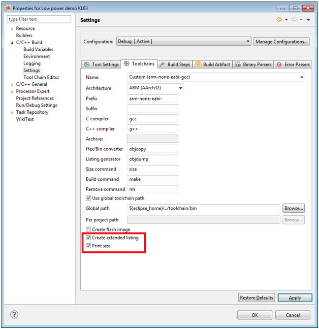
If you want to know details of compiled code and the code size, you can use the following options to create extended list file and print code size info on the following Toolchains tab: |
You can generate Processor Expert code and process Build of the application without any error and warning.
When the Build is finished the following information is provided in the Console window:
'Invoking: Cross ARM GNU Create Listing'
arm-none-eabi-objdump --source --all-headers --demangle --line-numbers --wide "Low power demo KL03.elf" > "Low power demo KL03.lst"
'Finished building: Low power demo KL03.lst'
' '
'Invoking: Cross ARM GNU Print Size'
arm-none-eabi-size --format=berkeley "Low power demo KL03.elf"
text data bss dec hex filename
8860 112 640 9612 258c Low power demo KL03.elf
'Finished building: Low power demo KL03.siz'
Routing of pins
When you open the gpio_pins component (in Component Inspector window) you can see that there are configured pins that are already used on target board:
- SW2 - ADC0_SE9/PTB0/IRQ_5/LLWU_P4/EXTRG_IN/SPI0_SCK/I2C0_SCL – input pin for the SW2 button on the board
- SW3 - ADC0_SE1/CMP0_IN1/PTB5/IRQ_12/TPM1_CH1/NMI_b - input pin for the SW3 button on the board
- ACCEL_INT - ADC0_SE0/CMP0_IN0/PTA12/IRQ_13/LPTMR0_ALT2/TPM1_CH0/TPM_CLKIN0/CLKOUT – input pin of inertial sensor interrupt
- LED_RED - PTB10/TPM0_CH1/SPI0_SS_b – output pin that driver the red LED of the RGB LED on the board
- LED_GREEN - PTB11/TPM0_CH0/SPI0_MISO - output pin that driver the green LED of the RGB LED on the board
- LED_BLUE - PTB13/CLKOUT32K/TPM1_CH1/RTC_CLKOUT - output pin that driver the blue LED of the RGB LED on the board
Note:
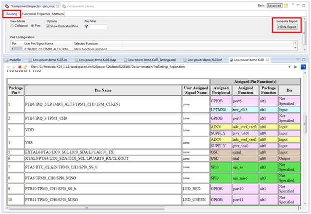
You can see routing of all pins when you generate report of PinSettings component. Open the Component Inspector of PinSettins, Routing tab and click on the HTML Report button.
We will use the SW2 button to wakeup the CPU and the green LED for indication of the CPU state.
Adding Processor Expert components
Now you can add all components for the low power demo application.
- Init_LLWU and fsl_llwu_hal components to control LLWU device
- Init_SRTC and fsl_rtc_hal to control RTC device
- Init_LPTMR and fsl_lptmr_hal to control LPTMR device
- fsl_smc_hal to control SMC (System Mode Controller) device
CPU device
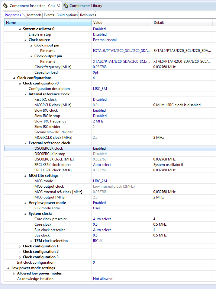
We are going to use external oscillator 32768Hz and we need to configure device to allow Very Low Leakage Stop modes. There are set following properties in the Component Inspector of the CPU (switch to Advance view):
- Check that the Clock settings/Clock Sources/System oscillator 0 property is Enabled and set Enable in stop property to Enabled. The Clock source, clock pins and clock frequency are preset for the FRDM-KL03Z board.
- Go to the Clock configuration/Clock Configuration 0 and set:
- Internal reference clock/Slow IRC frequency to 2MHz (it is enough for our demo application and it also decreases power consumption).
- MCG lite settings/MCG mode set to LIRC_2M
- Very low power mode to Enabled (leave setting of VLP mode entry to User because the VLLS1 mode is entered after blinking; we will write the code to enter VLLS1 mode)
- System clocks/Core clock set to 0.5Mhz
- System clocks/Bus clock set to 0.5Mhz (it allow us to enter very low leakage stop modes)
- Set Low Power mode settings/Acknowledge isolation to Not allowed value (we will do it in the user code)
LLWU (Low-Leakage Wakeup unit) device
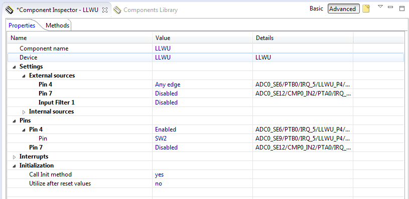
Open the Component Inspector of Init_LLWU, switch to Advance view and set following properties:
- Set Settings/External Source/Pin 4 to Any edge value (we will use this pin that is connected to SW2 button)
- Set Pins/Pin 4 to Enabled and select SW2 in the item below
- Set Initialization/Utilize after reset values to no
We will use the LLWU to wake-up the CPU and we need not any interrupt.
RTC (Real Time Clock) device
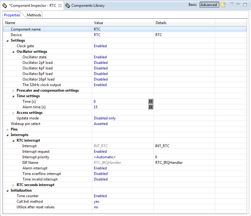
Open the Component Inspector of Init_SRTC, switch to Advance view and set following properties:
- Set Settings/Clock gate to Enabled
- Set Settings/Oscillator settings/Oscillator state to Enabled (it enables external oscillator also in stop modes)
- Set Settings/Time settins/Alarm time [s] to 15 (15 seconds timeout to wake-up from VLLS1 mode)
- Set Interrupts/ RTC interrupt/Interrupt request to Enabled
- Set Interrupts/ RTC interrupt/Time overflow interrupt to Disabled
- Set Interrupts/ RTC interrupt/Time invalid interrupt to Disabled
- Set Initialization/Time counter to Enabled
- Set Initialization/Utilize after reset values to no
LPTMR (Low-Power Timer) device
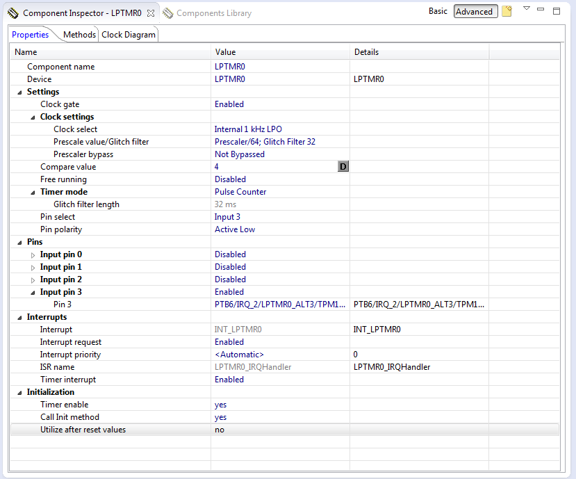
Open the Component Inspector of Init_LPTMR, switch to Advance view and set following properties:
- Set Settings/Clock gate to Enabled
- Set Settings/Clock settings/Clock select to Internal 1kHz LPO (this clock source is enabled in the VLLS1 mode)
- Set Settings/Clock settings/Prescale value/Glitch filter to Prescaler/64; Glitch Filter 32 (it will eliminates glitches on connected button that will be used for generating pulses)
- Set Settings/Compare value to 4 (the LPTMR interrupt is invoked when the compare value is equal to counter and the counter value is increased, i.e. 5 pulses on the input pins invoke the LPTMR interrupt)
- Set Settings/Timer mode to Pulse Counter (we will use the timer to count external pulses on the input pin 3)
- Set Settings/Pin select to Input 3
- Set Settings/Pin polarity to Active Low
- Set Pins/Input pin 3 to Enabled and select PTB6/IRQ_2/LPTMR0_ALT3/TPM1_CH1, TPM_CLKIN1 in Pin 3 item.
- Set Interrupts/Interrupt request to Enabled
- Set Interrupts/Timer interrupt to Enabled (we will use the timer interrupt to wake-up CPU from VLLS1 mode after 5 pulses on the input 3 pin)
- Set Initialization/Timer enable to yes
- Set Initialization/Utilize after reset values to no
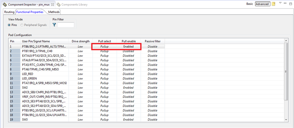
To avoid glitches on the PTB6 pin, that is used as input pin of the LPTMR, we will also enable pull-up in the PinSettins. Open Component Inspector of the PinSettings, select Functional Properties tab and set the pin number 1 (PTB6) as follows:
We have finished design time settings of Processor Expert components and we are ready to write the application code.
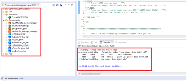
When you generate code and Build the application there will not be any error or warning. The Processor Expert project looks as follow:
Application code
During the component settings we have enabled two interrupts – RTC interrupt and LPTMR interrupt. Therefore we need to write theses interrupt service routines. If you look for example into RTC.h file, you can find the declaration of the RTC_IRQHandler interrupt routine. So we can use the declaration to write the definition of the routine in the main.c program module:
#define RTC_ALARM_TIMEOUT_SEC 15
#define LED_BLINK 5
/* RTC interrupt service routine */
PE_ISR(RTC_IRQHandler) {
if (RTC_HAL_HasAlarmOccured(RTC_BASE)) {
// set the next alarm in RTC_ALARM_TIMEOUT_SEC seconds (clear also the TAF flag)
RTC_HAL_SetAlarmReg(RTC_BASE,RTC_HAL_GetAlarmReg(RTC_BASE) + RTC_ALARM_TIMEOUT_SEC);
}
if (RTC_HAL_IsTimeInvalid(RTC_BASE)) {
/* clear TIF (Time Invalid Flag) by stop of the counter and setting TSR reg */
RTC_HAL_EnableCounter(RTC_BASE, false);
RTC_HAL_SetSecsReg(RTC_BASE, 0);
/* enable counter */
RTC_HAL_EnableCounter(RTC_BASE, true);
}
}
This interrupt routine services the Alarm interrupt in case that it is invoked during blinking of the green LED in the run mode (clear the flag and set the new Alarm time) and also it services the Invalid Time interrupt that can occur during recovering from the VLLS1 mode. Please note, that RTC module is little bit special, it runs in all run, wait and stop modes and the reset enables the Time Invalid interrupt bit (TIIE bit in RTC_IER) and invoke the Time Invalid interrupt on reset (POR or software reset). Therefore we need to clear the Invalid Time flag otherwise the application remain invoking RTC interrupt in an infinite cycle and the application does not work at all (it is also one of the issue that has not a straight forward solution). The RTC interrupt routine (defined above) shall properly serve all case we need in our application.
Please note, that RTC interrupt always cause the wake-up from low-leakage stops modes (it is not configurable by LLWU on KL03 derivatives – see the chip-specific LLWU information). In addition, the after reset value of RTC_SR register is 0x01 (TIF flag is set). Therefore when the RTC is not initialized and a low-leakage stop mode is entered the CPU is immediately woken-up due to the RTC module interrupt flag (TIF flag is set). I.e. you must always properly initialize RTC module and clear all flags before you enter a low-leakage stop mode.
We need also a service routine for the LPTMR device that is used for waking up from VLSS1 mode. This is a simple interrupt service routine that just clear the LPTMR interrupt flag:
/* LPTMR interrupt service routine */
PE_ISR(LPTMR0_IRQHandler) {
/* clear LPTMR interrupt flag */
LPTMR_HAL_ClearIntFlag(LPTMR0_BASE);
}
Now we can write the main() function. We will need a temporary count variables for blinking:
/* Write your local variable definition here */
volatile uint32_t i; // for waiting
uint8_t blink_count;
After devices initialization in PE_low_level_init() we need to check the reason of reset (POR reset or VLLS1 recovery). Thus we can write following code:
/* Write your code here */
if (RCM_SRS0 == 0x01) { /* test the reason of reset - wakeup on VLLS */
if(PMC->REGSC & PMC_REGSC_ACKISO_MASK) {
PMC->REGSC |= PMC_REGSC_ACKISO_MASK; /* VLLSx recovery */
}
for (blink_count = 0; blink_count < LED_BLINK; blink_count++) {
// green LED blinking
GPIO_DRV_ClearPinOutput(kGpioLED2);
//GPIOB_PCOR = (GPIOB_PCOR & (~GPIOB_PSOR_MASK)) | GPIOB_PSOR_VALUE;
for (i = 0; i<40000; i++);
GPIO_DRV_SetPinOutput(kGpioLED2);
//GPIOB_PSOR = (GPIOB_PSOR & (~GPIOB_PSOR_MASK)) | GPIOB_PSOR_VALUE;
for (i = 0; i<40000; i++);
}
// set the next alarm in "RTC_ALARM_TIMEOUT_SEC" seconds (clear also the TAF flag)
RTC_HAL_SetAlarmReg(RTC_BASE,RTC_HAL_GetAlarmReg(RTC_BASE)+RTC_ALARM_TIMEOUT_SEC);
} else {
/* power-on reset */
/* switch the green LED on */
GPIO_DRV_ClearPinOutput(kGpioLED2);
/* wait a while */
for (i = 0; i<40000; i++);
/* switch the green LED off */
GPIO_DRV_SetPinOutput(kGpioLED2);
}
In case of VLLS1 recovery we acknowledge the pin isolation ACKISO bit in the PMC_REGSC register. This bit must be cleared to allow normal run mode of all pins. Then five blinking of the green LED follows (it is just a simple code for demo purposes only; you can write your own more sophisticated code for blinking by TPMx device with Init_TPM component if you want).
In case of POR reset one blink of the green LED is processed.
When the reset/wake-up state is served by our application code the VLLS1 mode can be entered. As the first step, we need to be sure that there are not any interrupt flags set to wake-up the CPU from VLLS1 mode so we clear LLWU and SW2 pin (PTB0) interrupt flags and then we enter VLLS1 mode by using enter_vllsx function:
/* clear LLWU flag for the selected pin 4 - PTB0 */
LLWU_F1 |= LLWU_F1_WUF4_MASK;
/* clear interrupt flag of the SW2 pin - PTB0 */
PORTB_PCR0 |= PORT_PCR_ISF_MASK;
// enter the VLLS3
//enter_vllsx((smc_por_option_t)NULL,kSmcStopSub3);
// enter the VLLS0 - RTC and LPTMR do not work becuase of external crystal clock source does not work in the VLLS0 mode
//enter_vllsx(kSmcPorEnabled, kSmcStopSub0);
// enter the VLLS1
enter_vllsx((smc_por_option_t)NULL,kSmcStopSub1);
// switch the green LED on - error state when the VLLSx mode is not entered
GPIO_DRV_ClearPinOutput(kGpioLED2);
There is also code for switching on the green LED in case the VLLS1 mode is not entered (indication of the error state).
The enter_vllsx function is defined by the following way (it is used existing function from a demo KSDK demo example):
/*
* VLLSx mode entry routinue
*/
static void enter_vllsx(smc_por_option_t PORPOValue, smc_stop_submode_t VLLSValue) {
smc_power_mode_config_t smcConfig;
/* set power mode to specific VLLSx mode */
smcConfig.porOption = true;
smcConfig.porOptionValue = (smc_por_option_t) PORPOValue;
smcConfig.powerModeName = kPowerModeVlls;
smcConfig.stopSubMode = (smc_stop_submode_t) VLLSValue;
SMC_HAL_SetMode(SMC_BASE, &smcConfig);
}
It is all code we need for our low power demo application. The application can be built and run now.
Debugging
The application does not contain any debug connection by default in KDS 1.1.1. The KDS 2.0.0 contains debug configurations but the settings must be updated according to following description. We just need to add (modify) a debug configuration for our FRDM-KL03Z board and Open SDA Segger j-link debugger.
Open the context menu of the Low power demo KL03 project in the Project Explorer window and select Debug As > Debug Configurations ....
In the Debug Configuration window double click on the GDB SEGGER J-Link Debugger item and a new Low power demo KL03 Debug configuration is created.
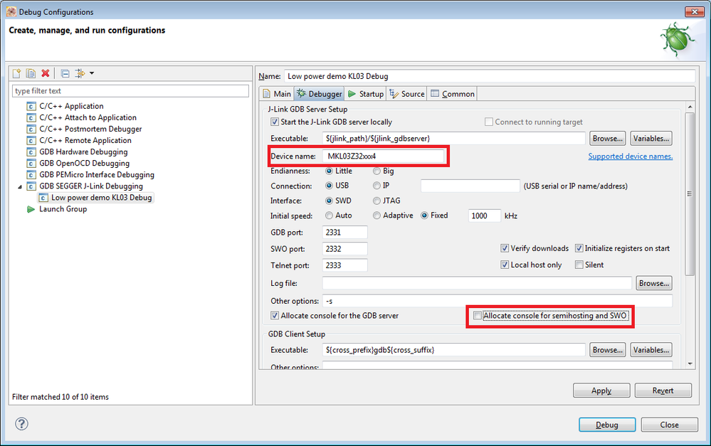
Select the Debugger tab and enter the Device name: MKL03Z32xxx4 (you can find the correct CPU name in list when you open Support device names link that is located to right of this item). Uncheck Allocate console for semihosting and SWO (SWO is not support by OpenSDA SEGGER J-link).
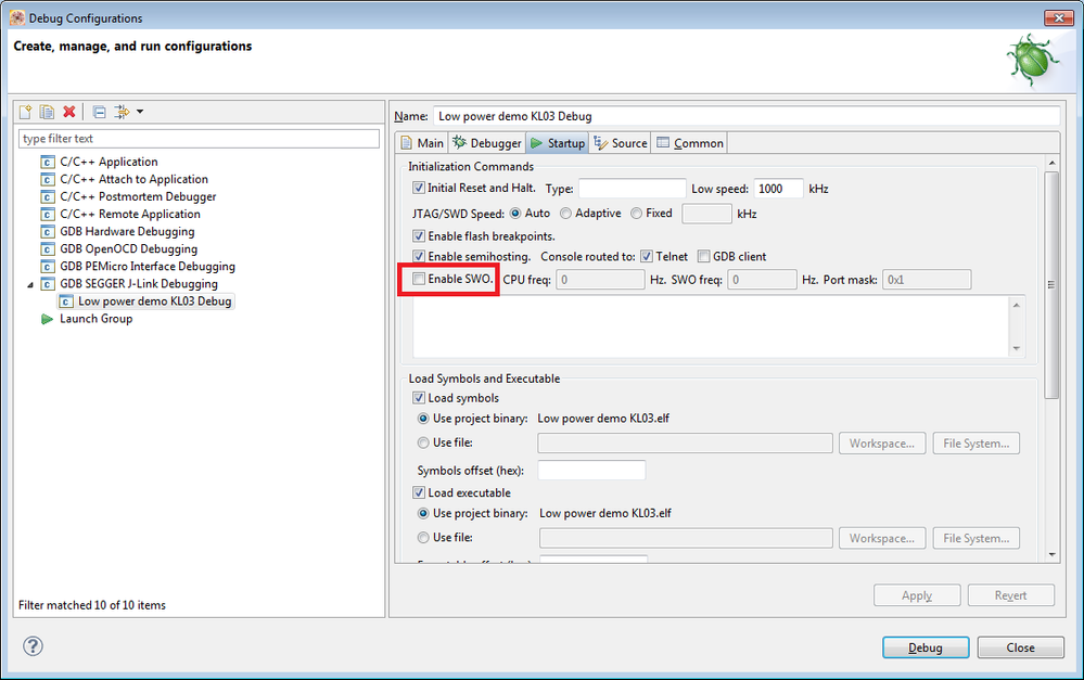
Go to on Startup tab and uncheck the Enable SWO option (SWO is not supported by OpenSDA SEGGER J-link).
Click on the Apply and Debug button and the debugger starts (you must have the FRDM-KL03Z board connected to the workstation).
You can now start the application (click on the Resume button) and check the functionality. The debugger is disconnected due to VLLS1 mode entry. But the application run and can be used.
If you want to connect a button for the LPTMR pulses generating you can connect one pin of the button to the PTB6 on pin #4 of 8-pins connector J1 and the second pin of the button to the GND to the pin #7 of the 10-pins connector J2, see below:
You can use this demo application as a start point of your real low power application. I hope it will help you and save your time of your first low power application implementation in the Processor Expert.
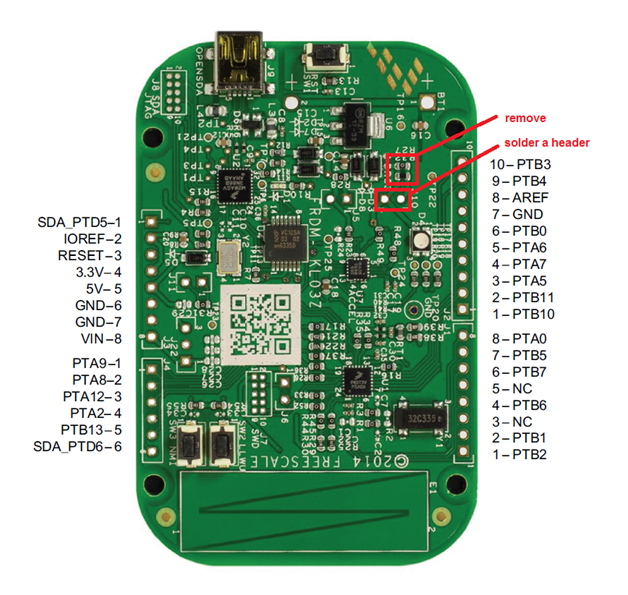
There is also possible to measure power consumption of the CPU in VLLS1 mode. It is described in the FRDM-KL03 User Guide. Just unsolder R27 and R28 and solder a header pins to J10 position of the board. You must use jumper for J10 now to connect power supply for the CPU and when the jumper is removed you can use these two pins to measure the energy consumption of the CPU (e.g. by a multimeter).
- Mark as Read
- Mark as New
- Bookmark
- Permalink
- Report Inappropriate Content
Hello,
This example was very helpful. I wondered if it would be possible to get the full C code since I don't use the Component Inspector?
Also, from what I've read, an interrupt cannot cause a wake-up from VLLSx modes...should be only enabled from an LLWU input source or the Reset pin, according to the User's manual, Chp.15, table 15-7. In this code, you are clearly waking from VLLS1 using the LPTMR interrupt. Does this really work? If so, is VLLS1 the only mode that allows this or do others?
Thanks,
Sara

