- Forums
- Product Forums
- General Purpose MicrocontrollersGeneral Purpose Microcontrollers
- i.MX Forumsi.MX Forums
- QorIQ Processing PlatformsQorIQ Processing Platforms
- Identification and SecurityIdentification and Security
- Power ManagementPower Management
- Wireless ConnectivityWireless Connectivity
- RFID / NFCRFID / NFC
- MCX Microcontrollers
- S32G
- S32K
- S32V
- MPC5xxx
- Other NXP Products
- S12 / MagniV Microcontrollers
- Powertrain and Electrification Analog Drivers
- Sensors
- Vybrid Processors
- Digital Signal Controllers
- 8-bit Microcontrollers
- ColdFire/68K Microcontrollers and Processors
- PowerQUICC Processors
- OSBDM and TBDML
- S32M
-
- Solution Forums
- Software Forums
- MCUXpresso Software and ToolsMCUXpresso Software and Tools
- CodeWarriorCodeWarrior
- MQX Software SolutionsMQX Software Solutions
- Model-Based Design Toolbox (MBDT)Model-Based Design Toolbox (MBDT)
- FreeMASTER
- eIQ Machine Learning Software
- Embedded Software and Tools Clinic
- S32 SDK
- S32 Design Studio
- GUI Guider
- Zephyr Project
- Voice Technology
- Application Software Packs
- Secure Provisioning SDK (SPSDK)
- Processor Expert Software
-
- Topics
- Mobile Robotics - Drones and RoversMobile Robotics - Drones and Rovers
- NXP Training ContentNXP Training Content
- University ProgramsUniversity Programs
- Rapid IoT
- NXP Designs
- SafeAssure-Community
- OSS Security & Maintenance
- Using Our Community
-
- Cloud Lab Forums
-
- Knowledge Bases
- ARM Microcontrollers
- i.MX Processors
- Identification and Security
- Model-Based Design Toolbox (MBDT)
- QorIQ Processing Platforms
- S32 Automotive Processing Platform
- Wireless Connectivity
- CodeWarrior
- MCUXpresso Suite of Software and Tools
- MQX Software Solutions
-
- Home
- :
- RFID / NFC
- :
- NFC
- :
- Problem Reading Mifare cards on PN532 Customized board.
Problem Reading Mifare cards on PN532 Customized board.
Problem Reading Mifare cards on PN532 Customized board.
Antenna pn532 NXP
I have customized my own PN532 board.
1. For first assembly the board was working some time and some time it did not.(was getting i2c address , card read some time and other time it did not read the i2c address).without ground tap in antenna
2. Second time same board i assembled i am able to read i2c every time. but it is not able to read any card.
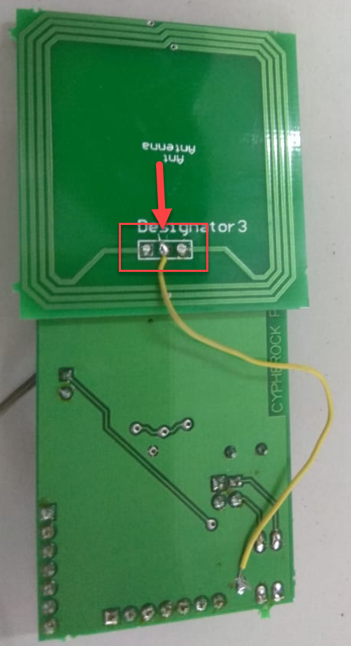
i tried nfc energy harvesting ic so without ground tap on antenna it showed no power, led glowed very less. then i ground tapped antenna so i was able to get full glow on LED on board energy harvesting ic. but still not able to read cards.
attaching the Schematic and board image
Hello,
Please help us to provide more information on below questions:
1. May I ask what is the purpose of the yellow wire in front of the antenna?
2. Is this connected to a ground plane in the antenna on an inner layer?
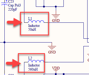
3. Why are the inductors different, or is this a typo?
Best regards,
Ivan.
Hii Ivan
Hello,
Please remove the ground from the antenna, only the matching circuit is ok to ground it. Please measure the antenna parameters with a Network analyzer e.g. a MiniVNA and match it correctly to the front-end so that it is correctly tuned at 13,56 MHz. Also please refer to the antenna design guide available in the following link: https://www.nxp.com/docs/en/application-note/AN1445_An1444.zip
Best regards,
Ivan.
Hii Ivan
1. The yellow wire is used to connect antenna ground tap to board ground
that is VSS.
2. Its a double side PTH board no inner layer.
3. Its a typo value 560nh both.( i have corrected in schematic after
attaching the files)
Also i wanted to ask they are TVSS1 AND TVSS2 transmitter ground on chip
different from other ground(VSS). should i use them for antenna ground
tapping while not shorting it to VSS (keeping them separate)
Thanks
Anmol Kohli
BTech-2016 Electronics Engineer
Embedded Design Engineer
m:+91-9958811944 e: anmol.workmails@gmail.com

