- Forums
- Product Forums
- General Purpose MicrocontrollersGeneral Purpose Microcontrollers
- i.MX Forumsi.MX Forums
- QorIQ Processing PlatformsQorIQ Processing Platforms
- Identification and SecurityIdentification and Security
- Power ManagementPower Management
- Wireless ConnectivityWireless Connectivity
- RFID / NFCRFID / NFC
- Advanced AnalogAdvanced Analog
- MCX Microcontrollers
- S32G
- S32K
- S32V
- MPC5xxx
- Other NXP Products
- S12 / MagniV Microcontrollers
- Powertrain and Electrification Analog Drivers
- Sensors
- Vybrid Processors
- Digital Signal Controllers
- 8-bit Microcontrollers
- ColdFire/68K Microcontrollers and Processors
- PowerQUICC Processors
- OSBDM and TBDML
- S32M
- S32Z/E
-
- Solution Forums
- Software Forums
- MCUXpresso Software and ToolsMCUXpresso Software and Tools
- CodeWarriorCodeWarrior
- MQX Software SolutionsMQX Software Solutions
- Model-Based Design Toolbox (MBDT)Model-Based Design Toolbox (MBDT)
- FreeMASTER
- eIQ Machine Learning Software
- Embedded Software and Tools Clinic
- S32 SDK
- S32 Design Studio
- GUI Guider
- Zephyr Project
- Voice Technology
- Application Software Packs
- Secure Provisioning SDK (SPSDK)
- Processor Expert Software
- Generative AI & LLMs
-
- Topics
- Mobile Robotics - Drones and RoversMobile Robotics - Drones and Rovers
- NXP Training ContentNXP Training Content
- University ProgramsUniversity Programs
- Rapid IoT
- NXP Designs
- SafeAssure-Community
- OSS Security & Maintenance
- Using Our Community
-
- Cloud Lab Forums
-
- Knowledge Bases
- ARM Microcontrollers
- i.MX Processors
- Identification and Security
- Model-Based Design Toolbox (MBDT)
- QorIQ Processing Platforms
- S32 Automotive Processing Platform
- Wireless Connectivity
- CodeWarrior
- MCUXpresso Suite of Software and Tools
- MQX Software Solutions
- RFID / NFC
- Advanced Analog
-
- NXP Tech Blogs
- Home
- :
- Product Forums
- :
- MPC5xxx
- :
- Question about SPI_1 module can not output signal at PIN PA[6](clock) and PA[7](MOSI) in S32R274
Question about SPI_1 module can not output signal at PIN PA[6](clock) and PA[7](MOSI) in S32R274
- Subscribe to RSS Feed
- Mark Topic as New
- Mark Topic as Read
- Float this Topic for Current User
- Bookmark
- Subscribe
- Mute
- Printer Friendly Page
- Mark as New
- Bookmark
- Subscribe
- Mute
- Subscribe to RSS Feed
- Permalink
- Report Inappropriate Content
Hi
The S32R274 has two SPI devices: SPI_1 and SPI_2, and there is no difference in the RM description.
I found that using the same SPI and pin(SIUL2) register configuration, other pins can output clock and data signals, but PA [6] and PA [7] cannot output signals, as shown in the following table:
PIN | Module | function | Register value | OUTPUT |
PA[6] | SPI_1 | SCK | 0x12840001 | Without output signal |
PB[2] | 0x12840004 | Output clock signal | ||
PA[7] | MOSI | 0x12840001 | Without output signal | |
PA[9] | 0x12840004 | Output data signal | ||
PA[0] | SPI_2 | SCK | 0x12840002 | Output clock signal |
PA[11] | 0x12840001 | Output clock signal | ||
PA[1] | MOSI | 0x12840002 | Output data signal | |
PA[12] | 0x12840001 | Output data signal |
SPI_1 supports the following pins:
CLK: PA [6], PB [2]
MOSI: PA [7], PA [9]
MISO: PA [8], PB [3], PH [7]
SPI_2 supports the following pins:
CLK: PA [0], PA [11]
MOSI: PA [1], PA [12]
MISO: PA [2], PA [13]
Chip selections pins and data input pins are not listed.
When use any SPI_2 configuration or SPI_1 use PB[2] as clock and PA[9] as output, the signal is normal, but PA[7] and PA[6] cannot output signal under the same configuration.
I used the correct pin register MSCR and SPI register configuration according to the reference manual, and I saw the register write the correct value in debug mode in real time.
Thanks!
Solved! Go to Solution.
- Mark as New
- Bookmark
- Subscribe
- Mute
- Subscribe to RSS Feed
- Permalink
- Report Inappropriate Content
Hi,
I did quick test on EVB and it works as expected, I can see nice signals on my scope. My test code is attached (copied from other projects, maybe some comments are not valid).
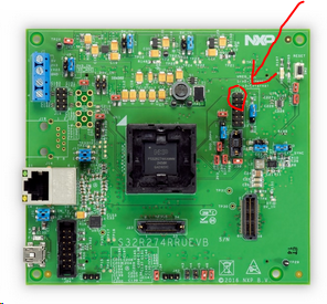
If you use EVB, PA6 and PA7 are available on J13 on the adapter:

Regards,
Lukas
- Mark as New
- Bookmark
- Subscribe
- Mute
- Subscribe to RSS Feed
- Permalink
- Report Inappropriate Content
- Mark as New
- Bookmark
- Subscribe
- Mute
- Subscribe to RSS Feed
- Permalink
- Report Inappropriate Content
- Mark as New
- Bookmark
- Subscribe
- Mute
- Subscribe to RSS Feed
- Permalink
- Report Inappropriate Content
Hi Lukas
Thank you very much, your test is right.
When I test again, I also observed the output signal in PA[6] and PA[7] by J13.
I already know the reason.
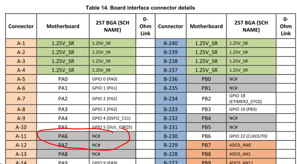
Only PA[8] PA[7] PA[6] in the MPC57XXXMB Evaluation Board Motherboard which I use to test did not connet to S32R274 corresponding pad.
So I only can observe the PA[6] PA[7] PA[8] output signal in Daughterboard J13.
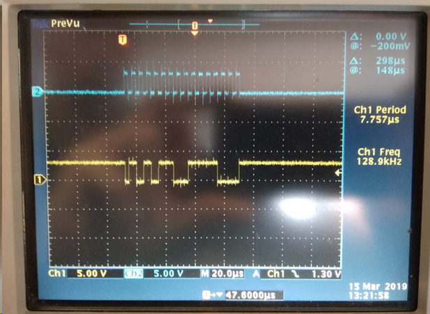
We can output SPI_1 signal in PA7[channel1], PA9[channel2], PA6[channel3] signal as follow:
Best Regards
Huaqiang
- Mark as New
- Bookmark
- Subscribe
- Mute
- Subscribe to RSS Feed
- Permalink
- Report Inappropriate Content
Hi Huaqiang,
it's mentioned in the user guide, section 5. Board interface connector:
https://www.nxp.com/docs/en/user-guide/S32R274-EVBUG.pdf

Regards,
Lukas
- Mark as New
- Bookmark
- Subscribe
- Mute
- Subscribe to RSS Feed
- Permalink
- Report Inappropriate Content
Hi Lukas
Thank you, I undrstand.
section 5. Board interface Connector is very useful for test signal.
Best Regards
Huaqiang
- Mark as New
- Bookmark
- Subscribe
- Mute
- Subscribe to RSS Feed
- Permalink
- Report Inappropriate Content
Hi David
This is the value of MSCR[n] register in S32R274 SIUL2 module, details as follow:
PIN | Module | function | Register | value | OUTPUT |
PA[6] | SPI_1 | SCK | SUIL2.MSCR[6] | 0x12840001 | Without output signal |
PB[2] | SUIL2.MSCR[18] | 0x12840004 | Output clock signal | ||
PA[7] | MOSI | SUIL2.MSCR[7] | 0x12840001 | Without output signal | |
PA[9] | SUIL2.MSCR[9] | 0x12840004 | Output data signal | ||
PA[0] | SPI_2 | SCK | SUIL2.MSCR[0] | 0x12840002 | Output clock signal |
PA[11] | SUIL2.MSCR[11] | 0x12840001 | Output clock signal | ||
PA[1] | MOSI | SUIL2.MSCR[1] | 0x12840002 | Output data signal | |
PA[12] | SUIL2.MSCR[12] | 0x12840001 | Output data signal |
Thank you
- Mark as New
- Bookmark
- Subscribe
- Mute
- Subscribe to RSS Feed
- Permalink
- Report Inappropriate Content
Hi, which register the table above points to?

