
- Forums
- Product Forums
- General Purpose MicrocontrollersGeneral Purpose Microcontrollers
- i.MX Forumsi.MX Forums
- QorIQ Processing PlatformsQorIQ Processing Platforms
- Identification and SecurityIdentification and Security
- Power ManagementPower Management
- Wireless ConnectivityWireless Connectivity
- RFID / NFCRFID / NFC
- Advanced AnalogAdvanced Analog
- Neural Processing UnitsNeural Processing Units
- MCX Microcontrollers
- S32G
- S32K
- S32V
- MPC5xxx
- Other NXP Products
- S12 / MagniV Microcontrollers
- Powertrain and Electrification Analog Drivers
- Sensors
- Vybrid Processors
- Digital Signal Controllers
- 8-bit Microcontrollers
- ColdFire/68K Microcontrollers and Processors
- PowerQUICC Processors
- OSBDM and TBDML
- S32M
- S32Z/E
-
- Solution Forums
- Software Forums
- MCUXpresso Software and ToolsMCUXpresso Software and Tools
- CodeWarriorCodeWarrior
- MQX Software SolutionsMQX Software Solutions
- Model-Based Design Toolbox (MBDT)Model-Based Design Toolbox (MBDT)
- FreeMASTER
- eIQ Machine Learning Software
- Embedded Software and Tools Clinic
- S32 SDK
- S32 Design Studio
- GUI Guider
- Zephyr Project
- Voice Technology
- Application Software Packs
- Secure Provisioning SDK (SPSDK)
- Processor Expert Software
- Generative AI & LLMs
-
- Topics
- Mobile Robotics - Drones and RoversMobile Robotics - Drones and Rovers
- NXP Training ContentNXP Training Content
- University ProgramsUniversity Programs
- Rapid IoT
- NXP Designs
- SafeAssure-Community
- OSS Security & Maintenance
- Using Our Community
-
- Cloud Lab Forums
-
- Knowledge Bases
- ARM Microcontrollers
- i.MX Processors
- Identification and Security
- Model-Based Design Toolbox (MBDT)
- QorIQ Processing Platforms
- S32 Automotive Processing Platform
- Wireless Connectivity
- CodeWarrior
- MCUXpresso Suite of Software and Tools
- MQX Software Solutions
- RFID / NFC
- Advanced Analog
- Neural Processing Units
-
- NXP Tech Blogs
- RSS フィードを購読する
- トピックを新着としてマーク
- トピックを既読としてマーク
- このトピックを現在のユーザーにフロートします
- ブックマーク
- 購読
- ミュート
- 印刷用ページ

- 新着としてマーク
- ブックマーク
- 購読
- ミュート
- RSS フィードを購読する
- ハイライト
- 印刷
- 不適切なコンテンツを報告
I'm learning the example project of BlinkLED. And it runs well. However, the example is to make LED2 blink, then I'm trying to modify the code to make other LED blinking. (let's say LED1 as an example)
Original Code:(same as a tutorial)
void pitCh0Handler(void){
PIT_DRV_ClearStatusFlags(INST_PIT1, 0U); /* Clear PIT channel 0 interrupt flag */
SIUL2->GPDO[0] ^= SIUL2_GPDO_PDO_4n_MASK; / * Toggle LED (GPIO 0 connected to user LED 2) */
}
int main(void){
CLOCK_DRV_Init(&clockMan1_InitConfig0);
PINS_DRV_Init(NUM_OF_CONFIGURED_PINS, g_pin_mux_InitConfigArr);
INT_SYS_InstallHandler(PIT_Ch0_IRQn, &pitCh0Handler, NULL);
PIT_DRV_Init(INST_PIT1, &pit1_InitConfig);
PIT_DRV_InitChannel(INST_PIT1, &pit1_ChnConfig0);
PIT_DRV_StartChannel(INST_PIT1,0U);
}
Modify area:
change pin mux to PA[4], which represents LED1.
SIUL2->GPDO[4] ^= SIUL2_GPDO_PDO_4n_MASK
Result: LED1 turns on, but never blink.
Does anyone know why?
I think the problem is "SIUL2_GPDO_PDO_4n_MASK", but I couldn't find any pin muxing in the MPC5748G datasheet!
No matter what I search ("SIUL", "GPDO", “GPDI”) inside the datasheet, I receive very limited information. Unlike MPC5744P datasheet, clear and helpful. Or am I looking at wrong data datasheet?
Please helps!
解決済! 解決策の投稿を見る。

 lukaszadrapa
- 新着としてマーク
- ブックマーク
- 購読
- ミュート
- RSS フィードを購読する
- ハイライト
- 印刷
- 不適切なコンテンツを報告
See the description of GPDO register. It's 32bit register which contains four bits to control four pins.
So, GPDO[0] covers GPIOs 0-3. GPDO[1] covers GPIOs 4-7 and so on...
To write PA[4], you need to write GPDO[1] using mask SIUL2_GPDO_PDO_4n_MASK.
(Note: this depends on used header file. Sometimes the GPDO is defined as array of 32bit registers like this, sometimes it's defined as array of 8bit registers, so it is more straightforward. Both options can be used.)
Anyway, if you use SDK, why not to use SDK functions for this? There are functions like PIN_DRV_WritePin, PIN_DRV_SetPins, PIN_DRV_ClearPins, PIN_DRV_TogglePins...
Regards,
Lukas
lukaszadrapa
- 新着としてマーク
- ブックマーク
- 購読
- ミュート
- RSS フィードを購読する
- ハイライト
- 印刷
- 不適切なコンテンツを報告
Hi Junyi,
description of the registers and pin muxing can be found in the reference manual:
https://www.nxp.com/webapp/Download?colCode=MPC5748GRM
There's an excel file attached inside the document:
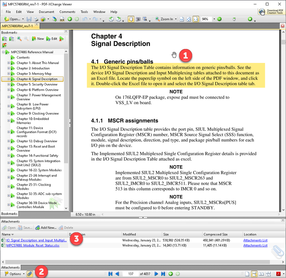
Regards,
Lukas
- 新着としてマーク
- ブックマーク
- 購読
- ミュート
- RSS フィードを購読する
- ハイライト
- 印刷
- 不適切なコンテンツを報告
Lukas,
Thank you for your reply.
I found the excel, but it didn't solve my question.
For LED2[PA0]:
SIUL2_GPDO_PDO_4n_MASK = 0x01000000
then how to map the LED1[PA4]? To make it turn on?
Thanks.
lukaszadrapa
- 新着としてマーク
- ブックマーク
- 購読
- ミュート
- RSS フィードを購読する
- ハイライト
- 印刷
- 不適切なコンテンツを報告
See the description of GPDO register. It's 32bit register which contains four bits to control four pins.
So, GPDO[0] covers GPIOs 0-3. GPDO[1] covers GPIOs 4-7 and so on...
To write PA[4], you need to write GPDO[1] using mask SIUL2_GPDO_PDO_4n_MASK.
(Note: this depends on used header file. Sometimes the GPDO is defined as array of 32bit registers like this, sometimes it's defined as array of 8bit registers, so it is more straightforward. Both options can be used.)
Anyway, if you use SDK, why not to use SDK functions for this? There are functions like PIN_DRV_WritePin, PIN_DRV_SetPins, PIN_DRV_ClearPins, PIN_DRV_TogglePins...
Regards,
Lukas
- 新着としてマーク
- ブックマーク
- 購読
- ミュート
- RSS フィードを購読する
- ハイライト
- 印刷
- 不適切なコンテンツを報告
Thanks!!!
GPDO[1] works! "SIUL2->GPDO[1] ^= SIUL2_GPDO_PDO_4n_MASK;"
I try to use function "PIN_DRV_TogglePins" to replace the mask(which I'm not familiar with), I found it is much easier for me to achieve the same result.
"PINS_DRV_TogglePins(PTA,1<<4);"
Again, Thank you for your help.
