- Forums
- Product Forums
- General Purpose MicrocontrollersGeneral Purpose Microcontrollers
- i.MX Forumsi.MX Forums
- QorIQ Processing PlatformsQorIQ Processing Platforms
- Identification and SecurityIdentification and Security
- Power ManagementPower Management
- Wireless ConnectivityWireless Connectivity
- RFID / NFCRFID / NFC
- Advanced AnalogAdvanced Analog
- MCX Microcontrollers
- S32G
- S32K
- S32V
- MPC5xxx
- Other NXP Products
- S12 / MagniV Microcontrollers
- Powertrain and Electrification Analog Drivers
- Sensors
- Vybrid Processors
- Digital Signal Controllers
- 8-bit Microcontrollers
- ColdFire/68K Microcontrollers and Processors
- PowerQUICC Processors
- OSBDM and TBDML
- S32M
- S32Z/E
-
- Solution Forums
- Software Forums
- MCUXpresso Software and ToolsMCUXpresso Software and Tools
- CodeWarriorCodeWarrior
- MQX Software SolutionsMQX Software Solutions
- Model-Based Design Toolbox (MBDT)Model-Based Design Toolbox (MBDT)
- FreeMASTER
- eIQ Machine Learning Software
- Embedded Software and Tools Clinic
- S32 SDK
- S32 Design Studio
- GUI Guider
- Zephyr Project
- Voice Technology
- Application Software Packs
- Secure Provisioning SDK (SPSDK)
- Processor Expert Software
- Generative AI & LLMs
-
- Topics
- Mobile Robotics - Drones and RoversMobile Robotics - Drones and Rovers
- NXP Training ContentNXP Training Content
- University ProgramsUniversity Programs
- Rapid IoT
- NXP Designs
- SafeAssure-Community
- OSS Security & Maintenance
- Using Our Community
-
- Cloud Lab Forums
-
- Knowledge Bases
- ARM Microcontrollers
- i.MX Processors
- Identification and Security
- Model-Based Design Toolbox (MBDT)
- QorIQ Processing Platforms
- S32 Automotive Processing Platform
- Wireless Connectivity
- CodeWarrior
- MCUXpresso Suite of Software and Tools
- MQX Software Solutions
- RFID / NFC
- Advanced Analog
-
- NXP Tech Blogs
- Home
- :
- 汎用マイクロコントローラ
- :
- LPCマイクロコントローラ
- :
- Re: SPIFI Flash Booting information for LPC4367
SPIFI Flash Booting information for LPC4367
- RSS フィードを購読する
- トピックを新着としてマーク
- トピックを既読としてマーク
- このトピックを現在のユーザーにフロートします
- ブックマーク
- 購読
- ミュート
- 印刷用ページ
SPIFI Flash Booting information for LPC4367
- 新着としてマーク
- ブックマーク
- 購読
- ミュート
- RSS フィードを購読する
- ハイライト
- 印刷
- 不適切なコンテンツを報告
Hi ,
I am using LPC4367 controller based evaluation board OM13088. I an trying to create the project which will use external flash for downloading the code instead of on chip flash.
I have created the project which is attached. Please check and let me know whether it is the proper one or need some modification in the project created.
while debugging the code, I am getting below error,
MCUXpresso IDE RedlinkMulti Driver v11.2 (Sep 22 2020 13:23:35 - crt_emu_cm_redlink build 19)
Found chip XML file in C:/Gaurav More/Project/New Feeder Relay/F4/SourceCode/CPU/TestCode/SPIFI_BOOT_2/Test_SPIFI_Prj/Debug\LPC4337.xml
Reconnected to existing LinkServer process.
Probe Firmware: LPC-LINK2 CMSIS-DAP V5.361 (NXP Semiconductors)
Serial Number: BSARBQEQ
VID:PID: 1FC9:0090
USB Path: \\?\hid#vid_1fc9&pid_0090&mi_00#8&11bf0f26&0&0000#{4d1e55b2-f16f-11cf-88cb-001111000030}
Using memory from core 0 after searching for a good core
debug interface type = Cortex-M3/4 (DAP DP ID 2BA01477) over SWD TAP 0
processor type = Cortex-M4 (CPU ID 00000C24) on DAP AP 0
number of h/w breakpoints = 6
number of flash patches = 2
number of h/w watchpoints = 4
Probe(0): Connected&Reset. DpID: 2BA01477. CpuID: 00000C24. Info: <None>
Debug protocol: SWD. RTCK: Disabled. Vector catch: Disabled.
Content of CoreSight Debug ROM(s):
RBASE E00FF000: CID B105100D PID 04000BB4C4 ROM (type 0x1)
ROM 1 E000E000: CID B105E00D PID 04000BB00C Gen SCS (type 0x0)
ROM 1 E0001000: CID B105E00D PID 04003BB002 Gen DWT (type 0x0)
ROM 1 E0002000: CID B105E00D PID 04002BB003 Gen FPB (type 0x0)
ROM 1 E0000000: CID B105E00D PID 04003BB001 Gen ITM (type 0x0)
ROM 1 E0040000: CID B105900D PID 04000BB9A1 CSt TPIU type 0x11 Trace Sink - TPIU
ROM 1 E0041000: CID B105900D PID 04000BB925 CSt ETM type 0x13 Trace Source - Core
NXP: LPC4337
DAP stride is 4096 bytes (1024 words)
Inspected v.2 External Flash Device on SPI LPC18_43_SPIFI_GENERIC.cfx
Image 'LPC18/43 Generic SPIFI Sep 25 2020 10:51:00'
Opening flash driver LPC18_43_SPIFI_GENERIC.cfx
Sending VECTRESET to run flash driver
Driver V.2 dynamic startup failed - driver Init provided no flash parameters
Flash Driver V.2 startup failed - rc Ef(55): Dynamic flash driver startup failed to provide flash parameters.
Terminate (0x0, 0x0, 0x0) status 0x40 - driver reports init failure - EXTSPI driver rc 13 - No supported SPIFI device found
chip initialization failed - Ef(55): Dynamic flash driver startup failed to provide flash parameters.
failed to initialize flash driver LPC18_43_SPIFI_GENERIC.cfx
Not able to get the reason for the same. since the SPIFI flash used in the Evaluation board is MX25L8035EM2I-10G.
Also I have one query.
while using internal flash the RAM allocated 32 KB for 1 core and 40 KB for other core and 16 KB for the third code as per the memory configuration, if we use the external flash then, What will be the to total size of the RAM used for execution?
Also it will be helpful if there is any reference code or a project since I tried to download the code from the below link but unable to download.
https://www.lpcware.com/content/faq/lpcxpresso/configuring-projects-multiple-flash
Request you to please share the code available in the above link.
Thanks
Gaurav More
- 新着としてマーク
- ブックマーク
- 購読
- ミュート
- RSS フィードを購読する
- ハイライト
- 印刷
- 不適切なコンテンツを報告
Hello @gauravmore
As you created a case for this application also , I am already providing you follow up there.
Many thanks
Diego.
- 新着としてマーク
- ブックマーク
- 購読
- ミュート
- RSS フィードを購読する
- ハイライト
- 印刷
- 不適切なコンテンツを報告
Hi Diego,
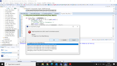
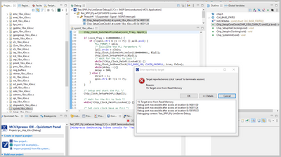
I have checked with the code modified as per the inputs received and referring the datasheet as well. After creating the project tried the debug but after programming the code in debug mode then it gives below mentioned errors. Also you can see it got stuck inside Chip_SetupCoreClock() function.
what could be the reason? since I made the changes in the hardware as well as per the below configuration
I am using OEM13088 evaluation board for further development. so please let me know with respect to the debug access in card of external flash. refer the source code attached in this thread
Thanks
Gaurav More
- 新着としてマーク
- ブックマーク
- 購読
- ミュート
- RSS フィードを購読する
- ハイライト
- 印刷
- 不適切なコンテンツを報告
Hi @gauravmore
Many thanks for your update!
Ok, After being able to flash the application . Then debugging and receiving those errors, as you are not able to execute main(), you have changed to Reset ISR , so this is the trace:
Test_SPIFI_Prj,->ResetISR()-> system_init() -> Board_SystemInit->Board_SetupClocking ->Chip_SetupCoreClock->Chip_Clock_CalcMainPLLValue() ,
So, in some place of the last function you get stuck at when writing or reading at any part of the CGU clocks related to the PLL , correct?
This seems very familiar to what other customers have faced at this thread:
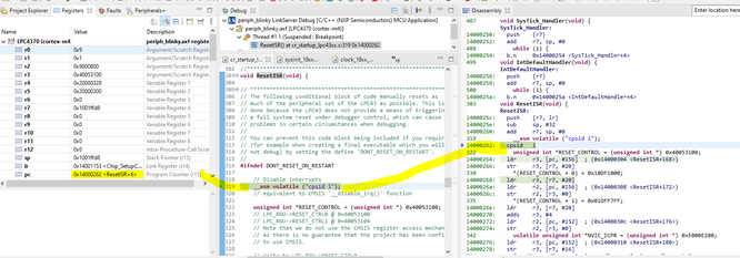
Other thing that may help is to check if all of this functions running from above the memory address for SPIFI of 0x1400_0000 ?
For example I use to check this using disassembly view and the processor PC.
Please accept my apologies for the delay.
Diego
- 新着としてマーク
- ブックマーク
- 購読
- ミュート
- RSS フィードを購読する
- ハイライト
- 印刷
- 不適切なコンテンツを報告
Hi Diego,
Thanks for the response,
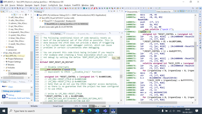
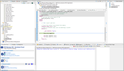
As per your input I also checked the same at my end. I have taken a screen shot of the same. Refer the below screen shot.
It is similar to what you have posted. But when I run the code, one more observation is there , this may help you since I am not able to make out. Refer the screen shot below,
Here you can see it show fail to execute for MI command, It seem that some how debugger is not able to read or access the QSPI flash.
Please check the same since we need to initiate the development based on it. Also one more query regarding the code,
As e know LPC43S67 is a flash less controller, it uses QSPI flash OEM13084. so Do we have some code or example code for this evaluation code so that I can get some hint.
Mean while I will refer the link you mentioned in the post
but there I didn't find any solution as such instead there are similar issues. I think NXP should give the example code for external flash based controllers.
Please check the same and let me know any more information regarding the same is required. also request you to check or test with the project which I have shared in the previous post in reply.
Have a nice day..
Thanks
Gaurav More
- 新着としてマーク
- ブックマーク
- 購読
- ミュート
- RSS フィードを購読する
- ハイライト
- 印刷
- 不適切なコンテンツを報告
Hi @gauravmore
Many thanks for your reply as well.
Just to verify , the project that you are currently debugging has the same settings than the one you previously attached in the post?
If not, could you share your current version ?
Best regards,
Diego
- 新着としてマーク
- ブックマーク
- 購読
- ミュート
- RSS フィードを購読する
- ハイライト
- 印刷
- 不適切なコンテンツを報告
Hi Deigo,
Thanks for the reply ,
Yes the code that I shared is same I have mode no changes in it. But still i will share the latest one as well for your reference,
I am using MCUXpresso V11.2 in which this project is created on OEM13088 evaluation board. By default there is another chip of Macronix (MX25L8035EM2I-10G) but I have replaced it with Winbond Chip (W25Q128JVFIM)
Thanks
Gaurav More
- 新着としてマーク
- ブックマーク
- 購読
- ミュート
- RSS フィードを購読する
- ハイライト
- 印刷
- 不適切なコンテンツを報告
Hi @gauravmore
Some updates, With my LPC4370 (flashless part) I was able to replicate your error.
I just changed project settings, and selected SPIFI .cfx drivers for run.
So I will come back to you as soon I gather more info.
All the best
Diego.
- 新着としてマーク
- ブックマーク
- 購読
- ミュート
- RSS フィードを購読する
- ハイライト
- 印刷
- 不適切なコンテンツを報告
Hi @gauravmore
I was able to jump to main application , by commenting out ( in a quick and dirty fashion) the Chip_Clock_DisableMainPLL() , which leads to the errors we have experimented , inside Chip_SetupCoreClock function.
it seems that the board init routines , do something that does not fit when we boot from a external flash. Yet , we will have to debug further this.
Therefore it seems that your project settings are ok, but we do not have the same LPC chips and the same boards ( I am actually using an LPC-Link 2 as a target ), Could you try from your side?
All the best
Diego.
- 新着としてマーク
- ブックマーク
- 購読
- ミュート
- RSS フィードを購読する
- ハイライト
- 印刷
- 不適切なコンテンツを報告
Hi Diego,
Thanks for the reply,
I modified the code as per your input and it is working. But only with debugger. After removing the debugger, I tried to boot then it is not booting. It should boot with external flash.
With debugger it is booting and code is running as per the expectation. I think some where we are missing some setting.
But I have one query, NXP should be having the sample code for LPC43S67 (OEM13084) for flash less code. since the evaluation board consists of flash less controller. There should be the codes which are tested ok in case of the this controller.
Mean while I will check the boot configuration from my side, but still if that configuration is wrong then also it should not run using the debugger right?
One more query: I was referring the code given in the below link,
https://www.lpcware.com/content/faq/lpcxpresso/configuring-projects-multiple-flash
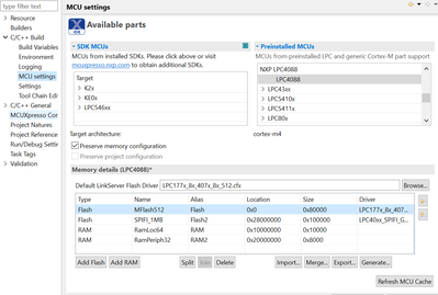
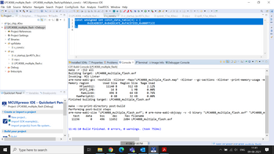
You have share the code for LPC4088. But in that code along with the M4 core SPIFI memory is also used,
So s per the input we can use it as a external memory but in this project I am not able to find the Allocation of the constant variable. But in the console it show that memory allocated,
need your help regarding the same. Since we also tryin this option in our application. Not able to find as in how this memory or the variable is allocated in the QSPIFI memory.
Please consider this as well.
Thanks
Gaurav More.
- 新着としてマーク
- ブックマーク
- 購読
- ミュート
- RSS フィードを購読する
- ハイライト
- 印刷
- 不適切なコンテンツを報告
Hi @gauravmore
Thank you for your input.
Upon my experience , even thought the MCU does not have the boot option for SPIFI selected, the debugger may still be able initiate a debug session. In your case, one simple hypothesis could be that the boot options pins do not have a fixed state for SPIFI ; and the MCU is booting in other option.
From my side I was able to run the project that you shared me after a POR and without a debugger. I just made minor modifications to make the LED Blinky on my LPC4370 board. Just for any reference ,please find my project attached.
I am currently checking with my team for more feedback regarding the comment to the Chip_Clock_DisableMainPLL() that we had to comment out to be able to jump to main() ; and also I am checking if we could provide an example for the LPC4367 that uses the an external flash memory to boot.
Regarding your second inquiry.
If we also want to statically allocate variables in the external flash memory, like the like const_data_table array from the example for the LPC4088:
I have some comments:
1 When we have multi-flash project, like the one for the LPC4088 , we can follow this tutorial Configuring projects to span multiple flash devices : you may use simplest way using the cr_section_macros.h directives or create your own linker script configuration.
2 From the image above , it can be seen that the const_data_table is allocated at the base address of the external flash . In contrast to applications that boot from a external flash , where the base address is used for the vector table.
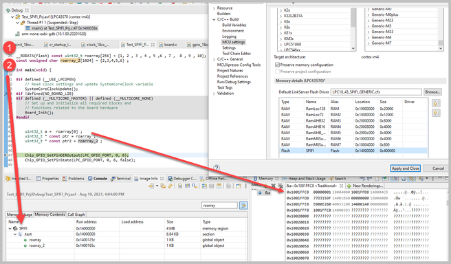
Here is a snapshot of me allocating two constant arrays in my project , that boots from the external flash. You can see how I am allocating the 2 arrays : the first one using the cr_section_macros.h RODATA directive ; and the second just declaring a constant array, since I only have one flash area the linker automatically allocates that array in the external flash.
The Image info window ,is also useful to know where our variables and functions are allocated.
I hope this could help you.
Diego.
- 新着としてマーク
- ブックマーク
- 購読
- ミュート
- RSS フィードを購読する
- ハイライト
- 印刷
- 不適切なコンテンツを報告
Hi Diego,
Thanks for the response and for the detailed information provided by you which will help us to proceed further.
In your case, one simple hypothesis could be that the boot options pins do not have a fixed state for SPIFI ; and the MCU is booting in other option. I think It could be the reason, I will check regarding the same. But still since you are using OEM13088 board can you share the Pin configuration done on the board? I Also did the same but still there might be some glitch,
Also regarding the allocation of the variable to the flash, in the given example of LPC4088 constant data is allocated in the Flash memory using __RODATA() attribute, in a similar manner can we assign the normal variable in the same area using the above attribute?
Main agenda behind this is Want to use generic flash driver and using that i want to use this SPIFI flash to store some critical variable with data in it instead of separately calling the read write function, similar to the SDRAM interface where we just need to initialize the EMI lines and then rest is taken care by the controller engine . Whenever we access the variable then it automatically use the EMI engine to access the address where the variable is stored.
Also Still as per the image below, it seems that you are viewing the axf file data, What I want is the place where this constant variable is assigned to the SPIFI address. Similar to the one you shared, __RODATA() attribute.
Also one more part,
If we use SPIFI boot mode the will we be losing the Tri core feature of the controller ?
What will be the total RAM memory available if we use the External flash boot and Internal RAM for code execution?
What is the method of allocating the normal variables in external flash, which will be updated periodically while running the application code?
Please provide the data required since I am not able to find the details regarding the same.
Thanks
Gaurav More
- 新着としてマーク
- ブックマーク
- 購読
- ミュート
- RSS フィードを購読する
- ハイライト
- 印刷
- 不適切なコンテンツを報告
Hi @gauravmore
Thanks for your reply
About : I think It could be the reason ( problems in Boot select pins ), I will check regarding the same. But still since you are using OEM13088 board can you share the Pin configuration done on the board? I Also did the same but still there might be some glitch
I am sorry for the late follow up, where you able to check whether you have any glitch problem? If you are still having issues could you share with me (in your internal ticket) your schematic settings? Also, do you have any setting in the flash OTP area?
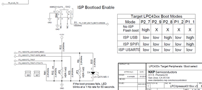
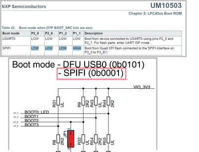
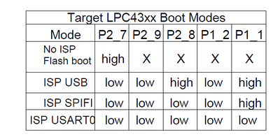
Unfortunately, I do not have an OEM13088 to test with me at home , due to Covid lockdown. I was actually programming the flash-less LPC4370 , from the LPC-Link 2 board OM13054. However , my boot configuration was the following
About : Also, regarding the allocation of the variable to the flash, in the given example of LPC4088 constant data is allocated in the Flash memory using __RODATA() attribute, in a similar manner can we assign the normal variable in the same area using the above attribute?
No, because RODATA is intended for constant variables . Check the below response.
About, What is the method of allocating the normal variables in external flash, which will be updated periodically while running the application code?
If from application execution you would like to modify an specific sector of flash to store critical data, you will need to include the SPIFI library for LPCXpresso. You can make use of the SPIFI library APIs to update sectors of the flash. Here is a tutorial on how to import the LPCSpifi library into the MCUXpresso ,that could help as a reference.
I will come back as soon as I can to reply all our pending inquires.
Many thanks for your patience.
Diego.
- 新着としてマーク
- ブックマーク
- 購読
- ミュート
- RSS フィードを購読する
- ハイライト
- 印刷
- 不適切なコンテンツを報告
Hi Diego,
Thanks for the reply,
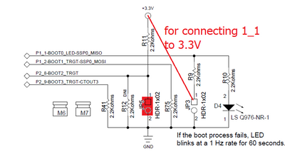
Yes till I am facing issue with respect to the booting of SPIFI. Also find the connection done at my side on OEM13088 eval board,
refer the attached schematic of the evaluation board as well.
About, What is the method of allocating the normal variables in external flash, which will be updated periodically while running the application code?
My expectation is , if assigned a variable in the external memory location and i simply called the variable and copied the data on to the variable, then will it simply copy? similar to the SDRAM behavior where once we initialize the EMI lines then automatically it works and functions?
Also I am expecting the method or and application note of assigning the Variable into the external flash.
Best Regards
Gaurav More
- 新着としてマーク
- ブックマーク
- 購読
- ミュート
- RSS フィードを購読する
- ハイライト
- 印刷
- 不適切なコンテンツを報告
Hi @gauravmore
I hope you are doing well , many thanks for your reply!
Regarding the MCU not being able to boot without a debug probe: I have not seem problems with your boot pin configuration. I think we may also take a closer look at the reset pin , to check whether it is affecting the boot process or not. Normally Debug probes handle the reset pin , and provide the required voltage and logic levels.
Another thing to review . From your source code I have seen that for the LED blink you called the function board LED set (to set pin state ), then you the toggle function:
   Board_LED_Set(0, true);
#endif
#endif
    // TODO: insert code here
    // Force the counter to be placed into memory
    volatile static int i = 0 ;
    // Enter an infinite loop, just incrementing a counter
    while(1) {

        __asm volatile ("nop");

        Board_LED_Toggle(1);
But I have not seen a call to the function Chip_GPIO_SetPinDIROutput() (to set the pin as an output). . When you are running with a debug session , are you able to see the LED blinking properly , right?
Regarding My expectation is , if assigned a variable in the external memory location and i simply called the variable and copied the data on to the variable, then will it simply copy?
Unfortunately , with the flash is different. it does not have the access properties than the SDRAM. When we need to write/read the flash from the application ; on many MCUs , to avoid data collision , it is required to run flash access routines from SRAM. For example the SPIFI Library provides APIs such as
spifi_program() or spifi_read(), below the definition of one of them,
/**
 * @brief	Program the device with the passed buffer
 * @param	pHandle		: Pointer to a LPCSPIFILIB device handle
 * @param	addr		: LPCSPIFILIB device address to start write at
 * @param	writeBuff	: Address of buffer to write, must be 32-bit aligned
 * @param	bytes		: Number of bytes to write
 * @return	A SPIFI_ERR_xxx error code (SPIFI_ERR_NONE is no errors)
 * @note	This function has no size limit. This function only works in blocking mode.
 */
SPIFI_ERR_T spifiProgram(const SPIFI_HANDLE_T *pHandle, uint32_t addr, const uint32_t *writeBuff, uint32_t bytes);
You mentioned that you are intending to store critical data on the flash. Do you want to avoid loosing critical data on a situation like a power loss or something similar?
BR,
Diego.
- 新着としてマーク
- ブックマーク
- 購読
- ミュート
- RSS フィードを購読する
- ハイライト
- 印刷
- 不適切なコンテンツを報告
Hi Diego,
Thanks for the reply and sorry for late response since i was in the mid of other issue related to the development.
But I have not seen a call to the function Chip_GPIO_SetPinDIROutput() (to set the pin as an output). . When you are running with a debug session , are you able to see the LED blinking properly , right?regarding the above query it is already there in the Board_Init() function named "Board_LED_Init()"
You mentioned that you are intending to store critical data on the flash. Do you want to avoid loosing critical data on a situation like a power loss or something similar? Yes i want to store the critical dare during power loss, regarding the other query I will elaborate more,
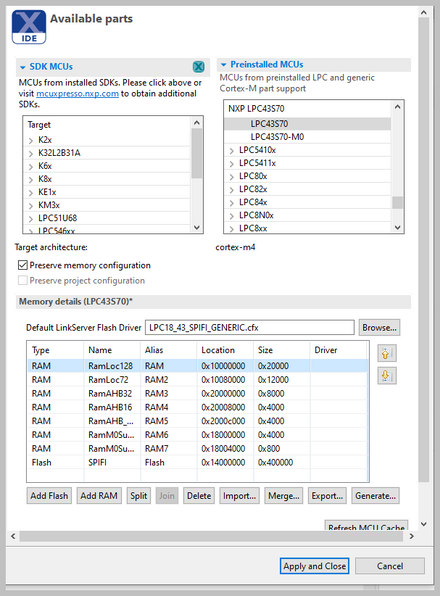
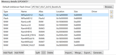
See I am developing and product there i have used SDRAM interface with LPC4367. Now the method i have used to interface and access is, I did the EMI initialization and then used added the SDRAM block in memory configuration section refer the screenshot below,
Now I used below method to allocate and access the variables in and from SDRAM,
__DATA(RAM8) S_Disturbance_Log g_st_DistubanceLog;g_st_DistubanceLog is a structure to store the critical information. And I am simply using the variable and when the variable is accessed then automatically it uses EMI lined to read and write the data to the variable allocated in that address.
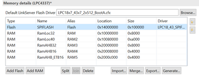
In the similar manner I want to use QSPI flash, where I have configured the flash drivers in the memory configuration section,
Now referring to the example code of LPC4088 I can see that there is a read only variable allocated and is it accessed in the code. But now is is possible to allocate the R/W variables so that I can assign the critical structure mentioned above in the flash memory directly since it will allocate the available space in the flash which reduces the efforts of specific assignment .
Let me know if it is clear to you or need some more details.
BR,
Gaurav More
- 新着としてマーク
- ブックマーク
- 購読
- ミュート
- RSS フィードを購読する
- ハイライト
- 印刷
- 不適切なコンテンツを報告
Hi @gauravmore
Many thanks for your reply, have some updates!
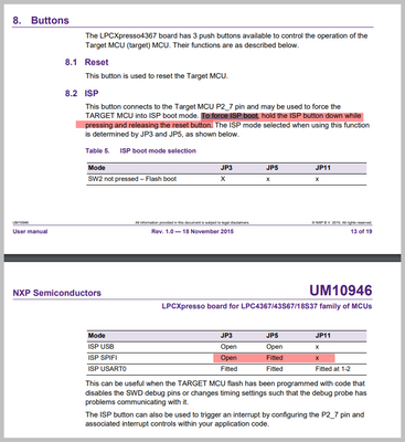
1 Regarding SPIFI boot without a debugger.
Today I tested ,with a colleague of mine, the attached project on the LPC43s67 OM13084. To boot with project and see the red LED blinking , we pressed the ISP button during reset and set the JP3 and JP5 according to the following snapshot from the OM , user guide. Let me know if it works for you.
2 Regarding the Chip_Clock_DisableMainPLL() that we had to comment in the startup routines to reach main() :
As I have been discussing with the AE team , that function actually disabled the PLL1; since the SPIFI peripheral clock was derived from the PLL1 path , disabling the PLL1 caused the failure you reported.
Therefore , what we need is to avoid the PLL1 from being disabled during startup Chip_SystemInit() routines. Unfortunately none of LPCopen drivers are not longer maintained, so we can adapt the startup routine to work properly and perform our desired clock settings. You may follow @cescvaro advice to refer to the 13.2.1.1 Changing the BASE_M4_CLK after power-up, reset, or deep power-down mode section of the UM.
3 Regarding the critical data structure.
My understanding (let me know if it is not accurate ) is that you want to save that critical data structure in the flash directly , and achieve R/W simplicity and fast access of SRAM allocation. As I mentioned earlier the external flash writes from the application require to be handled with the SPIFI library.
Therefore, to keep the simplicity of your application, although this is related to application design, I think in the following:
- Allocate critical data the SRAM, having an effortless and very fast access.
- Monitor the voltage level of your power source, and add something like a super-cap, in order to have extra energy when power is falling ( You can make use of the LPC43 BOD features) ; and when entering in the power loss scenario , put critical data into flash.
- Or every once in a while copy the critical data structure from SRAM from flash , using SPIFI library routines.
Let me hear from you if you succeeded to boot the application from SPIFI without a debugger.
All the best,
Diego.
- 新着としてマーク
- ブックマーク
- 購読
- ミュート
- RSS フィードを購読する
- ハイライト
- 印刷
- 不適切なコンテンツを報告
Hi Diego,
Thanks for the reply,
1. Regarding the SPIFI Boot issue, It worked after following the procedure you mentioned in the thread. Thanks a lot for the solution.
2. Regarding the Chip_Clock_DisableMainPLL() , Yes I will check with the inputs received from @cescvaro .
3. Regarding the SPIFI flash I got to know that we have to use the SPIFI library to read and write the critical data. But then will it work by simply including the SPIFI generic library in the MCU Setting section?
Also planning to use External SRAM instead of internal RAM for execution. Will check to used Internal Flash and external RAM provision for our development. Means for M4 Core use SRAM as a RAM and for M0App Core use internal RAM.
Let me know if it is possible.
Once again thanks for the solution for SPIFI Booting.
BR,
Gaurav More
- 新着としてマーク
- ブックマーク
- 購読
- ミュート
- RSS フィードを購読する
- ハイライト
- 印刷
- 不適切なコンテンツを報告
Hi Diego,
Thanks for the reply,
Yes I have received the files and download the same. Will check the same and revert.
Thanks
Gaurav More
- 新着としてマーク
- ブックマーク
- 購読
- ミュート
- RSS フィードを購読する
- ハイライト
- 印刷
- 不適切なコンテンツを報告
Hi Gaurav ,
I had a similar (maybe the same?) problem at startup the with an LPC4330 (it's flashless) and following some info like here https://community.nxp.com/t5/LPC-Microcontrollers/LPC4357-hard-fault-after-reset-from-application/m-... and here https://community.nxp.com/t5/LPC-Microcontrollers/LPC43xx-Chip-Clock-EnableCrystal-Hard-fault-adviso... I finally rewrote the Chip_SetupCoreClock following the datasheet at chapter about CGU "13.2.1 Configuring the BASE_M4_CLK for high operating frequencies" with some additional delay after some operation.
This worked for me:
void Chip_SetupCoreClock_new(CHIP_CGU_CLKIN_T clkin, uint32_t core_freq, bool setbase)
{
	/* 1 set IRC as base_M4_CLK source */
	PLL_PARAM_T ppll;
	uint32_t direct = 1;
	uint32_t i;
	//volatile uint32_t old_clk_src=0;

	//old_clk_src=(((LPC_CGU->PLL1_CTRL & 0x1F000000)) >> 24);	/* CLK_SEL [28:24] */

	if (clkin == CLKIN_CRYSTAL)
	{
		/* 2 Enable crystal */
		/* 3 wait 250 us    */
		Chip_Clock_EnableCrystal();
	}

	/* 4 should set autoblock bit */
	LPC_CGU->PLL1_CTRL |= (1<<11);

	/* reconfigure PL1 */
	/* M and N */
	ppll.srcin 		= CLKIN_IRC;
	ppll.autoblock 	= 1;			/* */

	Chip_Clock_CalcMainPLLValue(core_freq, &ppll);	/* calc of param for pll for desired freq - results in ppll !!!! */

	if (core_freq > 110000000UL)
	{
		if (!(ppll.ctrl & (1 << 7)) || ppll.psel)	/* NOT direct or PSEL != 0 --> PSEL is the divider, if > 0 means we are dividing */
		{
			direct = 0;
			PLL_PARAM_T lpll;
			/* Calculate the PLL Parameters */
			lpll.srcin = clkin;
			Chip_Clock_CalcMainPLLValue(110000000UL, &lpll);
			Chip_Clock_SetupMainPLL(&lpll);
		}
		else
		{
			direct = 1;	/* remember direct was set ! */
			ppll.ctrl &= ~(1 << 7);	/* clears for a moment */
			Chip_Clock_SetupMainPLL(&ppll);
			while(!Chip_Clock_MainPLLLocked()) {}
		}
	}
	else
	{
		Chip_Clock_SetupMainPLL(&ppll);
	}

	/* 5b select crystal as source for PLL1 */
	//if (clkin == CLKIN_CRYSTAL)
	{
		ppll.srcin = clkin;
		Chip_Clock_SetupMainPLL(&ppll);						/* set it */
	}

	/* 6 Wait for the PLL1 to lock */
	if (clkin == CLKIN_CRYSTAL)
	{
		while(!Chip_Clock_MainPLLLocked()) {}
	}

	/* 7 Select PLL1 p divider to 2 DIRECT = 0 PSEL = 0 */
	if (direct == 1)
	{
		ppll.ctrl &= ~(1<<7);	/* clears DIRECT */
		ppll.psel = 0;			/* psel to 0 */

	}
	Chip_Clock_SetupMainPLL(&ppll);	// yeah set again
	Chip_sysinit_delay(1000);				/* mine */
	while(!Chip_Clock_MainPLLLocked()) {}	/* mine */

	/* 8 Select PLL1 as BASE_M4_CLK source */
	Chip_Clock_SetBaseClock(CLK_BASE_MX, CLKIN_MAINPLL, true, false);	/* passing 3rd as true = AUTOBLOCK = true */

	/* 9 wait 50 us */
	Chip_sysinit_delay(0x4000);	/* 4800*/

	/* 10 Select PLL1 to direct output */
	if (direct == 1)
	{
		ppll.ctrl |= (1 << 7);	 /* set DIRECT */
		ppll.psel = 0;
		Chip_Clock_SetupMainPLL(&ppll); /* Set DIRECT to operate at full frequency */
	}

	Chip_sysinit_delay(1000);				/* mine */
	while(!Chip_Clock_MainPLLLocked()) {}	/* mine */

	if (setbase)
	{
		/* Setup system base clocks and initial states. This won't enable and
		   disable individual clocks, but sets up the base clock sources for
		   each individual peripheral clock. */
		for (i = 0; i < (sizeof(InitClkStates) / sizeof(InitClkStates[0])); i++)
		{
			Chip_Clock_SetBaseClock(InitClkStates[i].clk, InitClkStates[i].clkin,
									InitClkStates[i].autoblock_enab, InitClkStates[i].powerdn);
			Chip_sysinit_delay(1000);	/* mine */
		}
	}
}
and for Chip_Clock_EnableCrystal
/* Enables the crystal oscillator */
void Chip_Clock_EnableCrystal(void)
{
	volatile uint32_t delay;

	uint32_t OldCrystalConfig = LPC_CGU->XTAL_OSC_CTRL;

	/* Clear bypass mode */
	OldCrystalConfig &= (~2);
	if (OldCrystalConfig != LPC_CGU->XTAL_OSC_CTRL) {
		LPC_CGU->XTAL_OSC_CTRL = OldCrystalConfig;
	}

	/* Enable crystal oscillator */
	OldCrystalConfig &= (~1);
	if (OscRateIn >= 20000000)
	{
		OldCrystalConfig |= 4;	/* Set high frequency mode */

	}
	LPC_CGU->XTAL_OSC_CTRL = OldCrystalConfig;

	/* Delay for 250uSec */
	/*
	delay = 1000;
	while(delay--) {}
	*/
	for (delay = 0; delay < 100000 ; delay ++)
	{
		__NOP();
		__NOP();
	}
}
Let me know if it works for you.
regards,
fv
