- Forums
- Product Forums
- General Purpose MicrocontrollersGeneral Purpose Microcontrollers
- i.MX Forumsi.MX Forums
- QorIQ Processing PlatformsQorIQ Processing Platforms
- Identification and SecurityIdentification and Security
- Power ManagementPower Management
- Wireless ConnectivityWireless Connectivity
- RFID / NFCRFID / NFC
- Advanced AnalogAdvanced Analog
- MCX Microcontrollers
- S32G
- S32K
- S32V
- MPC5xxx
- Other NXP Products
- S12 / MagniV Microcontrollers
- Powertrain and Electrification Analog Drivers
- Sensors
- Vybrid Processors
- Digital Signal Controllers
- 8-bit Microcontrollers
- ColdFire/68K Microcontrollers and Processors
- PowerQUICC Processors
- OSBDM and TBDML
- S32M
- S32Z/E
-
- Solution Forums
- Software Forums
- MCUXpresso Software and ToolsMCUXpresso Software and Tools
- CodeWarriorCodeWarrior
- MQX Software SolutionsMQX Software Solutions
- Model-Based Design Toolbox (MBDT)Model-Based Design Toolbox (MBDT)
- FreeMASTER
- eIQ Machine Learning Software
- Embedded Software and Tools Clinic
- S32 SDK
- S32 Design Studio
- GUI Guider
- Zephyr Project
- Voice Technology
- Application Software Packs
- Secure Provisioning SDK (SPSDK)
- Processor Expert Software
- Generative AI & LLMs
-
- Topics
- Mobile Robotics - Drones and RoversMobile Robotics - Drones and Rovers
- NXP Training ContentNXP Training Content
- University ProgramsUniversity Programs
- Rapid IoT
- NXP Designs
- SafeAssure-Community
- OSS Security & Maintenance
- Using Our Community
-
- Cloud Lab Forums
-
- Knowledge Bases
- ARM Microcontrollers
- i.MX Processors
- Identification and Security
- Model-Based Design Toolbox (MBDT)
- QorIQ Processing Platforms
- S32 Automotive Processing Platform
- Wireless Connectivity
- CodeWarrior
- MCUXpresso Suite of Software and Tools
- MQX Software Solutions
- RFID / NFC
- Advanced Analog
-
- NXP Tech Blogs
- Home
- :
- 汎用マイクロコントローラ
- :
- LPCマイクロコントローラ
- :
- SPI SS required ?
SPI SS required ?
- RSS フィードを購読する
- トピックを新着としてマーク
- トピックを既読としてマーク
- このトピックを現在のユーザーにフロートします
- ブックマーク
- 購読
- ミュート
- 印刷用ページ
- 新着としてマーク
- ブックマーク
- 購読
- ミュート
- RSS フィードを購読する
- ハイライト
- 印刷
- 不適切なコンテンツを報告
We are using the LPC55S28 as an SPI Slave. It is the only device on the bus. During development we realized we needed another GPIO between devices. I attempted to change the SS to an input GPIO and was successful. Unfortunately, the SPI part stopped working when the GPIO was pulled high. Looking at Figure 119 and referring to paragraph 35.7.5 Slave Select of UM11126 Rev 2.1, it looks like the SS lines connect to the SPI state machine and are used to hold it into a known state.
The text says: "In slave mode, any asserted SSEL that is connected to a pin will activate the SPI. Does that mean that if there is no SSEL asserted that the SPI will become inactive?
If I were to design it I would have the SSEL reset the state machine since it is the beginning of a transfer sequence. That being said, is that how the internals are designed? If so, I will need to find another route to obtaining a set of I/O lines as this idea won't work.
解決済! 解決策の投稿を見る。
- 新着としてマーク
- ブックマーク
- 購読
- ミュート
- RSS フィードを購読する
- ハイライト
- 印刷
- 不適切なコンテンツを報告
> The text says: "In slave mode, any asserted SSEL that is connected to a pin will activate the SPI. Does that mean that if there is no SSEL asserted that the SPI will become inactive?
Exactly - this is the very intention behind the slave select signal.
The SS signal is only useful/required for multiple slave devices on one SPI master. If your connection involves only one master and one slave, you can disregard SS entirely, i.e. not use it in your configuration.
- 新着としてマーク
- ブックマーク
- 購読
- ミュート
- RSS フィードを購読する
- ハイライト
- 印刷
- 不適切なコンテンツを報告
Hi, Albert,
As the following Fig I copied from UM11126.pdf(for LPC552x), the FC0 has FC0_CTS_SDAX_SSEL0 and FC0_RTS_SCLX_SSEL1 pin, you have to set the FUNC bits in IOCON of P0_31 and P1_0 as 1, in this way, the FC0_CTS_SDAX_SSEL0 and FC0_RTS_SCLX_SSEL1 pin will function as slave chip select function: SPI0_SSEL0 and SPI0_SSEL1.
if you configure the FC0 as SPI. If the SPI0 is configured as slave mode, assume that the asserted logic of SPI0_SSELx is low, this is the pin state that the SPI0 functions as slave:
SPI0_SSEL0 SPI0_SSEL1 function
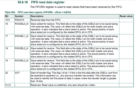
0 0 the SPI will function as salve, the SSEL0/SSEL1 state saved in FIFORD
0 1 the SPI will function as salve, the SSEL0/SSEL1 state saved in FIFORD
1 0 the SPI will function as salve, the SSEL0/SSEL1 state saved in FIFORD
1 1 the SPI will NOT function
If you want to both of GPIO and SPI slave work simultaneously, I suggest you choose another GPIO pin as GPIO function.
Hope it can help you

