- Forums
- Product Forums
- General Purpose MicrocontrollersGeneral Purpose Microcontrollers
- i.MX Forumsi.MX Forums
- QorIQ Processing PlatformsQorIQ Processing Platforms
- Identification and SecurityIdentification and Security
- Power ManagementPower Management
- MCX Microcontrollers
- S32G
- S32K
- S32V
- MPC5xxx
- Other NXP Products
- Wireless Connectivity
- S12 / MagniV Microcontrollers
- Powertrain and Electrification Analog Drivers
- Sensors
- Vybrid Processors
- Digital Signal Controllers
- 8-bit Microcontrollers
- ColdFire/68K Microcontrollers and Processors
- PowerQUICC Processors
- OSBDM and TBDML
- S32M
-
- Solution Forums
- Software Forums
- MCUXpresso Software and ToolsMCUXpresso Software and Tools
- CodeWarriorCodeWarrior
- MQX Software SolutionsMQX Software Solutions
- Model-Based Design Toolbox (MBDT)Model-Based Design Toolbox (MBDT)
- FreeMASTER
- eIQ Machine Learning Software
- Embedded Software and Tools Clinic
- S32 SDK
- S32 Design Studio
- GUI Guider
- Zephyr Project
- Voice Technology
- Application Software Packs
- Secure Provisioning SDK (SPSDK)
- Processor Expert Software
- MCUXpresso Training Hub
-
- Topics
- Mobile Robotics - Drones and RoversMobile Robotics - Drones and Rovers
- NXP Training ContentNXP Training Content
- University ProgramsUniversity Programs
- Rapid IoT
- NXP Designs
- SafeAssure-Community
- OSS Security & Maintenance
- Using Our Community
-
- Cloud Lab Forums
-
- Knowledge Bases
- ARM Microcontrollers
- i.MX Processors
- Identification and Security
- Model-Based Design Toolbox (MBDT)
- QorIQ Processing Platforms
- S32 Automotive Processing Platform
- Wireless Connectivity
- CodeWarrior
- MCUXpresso Suite of Software and Tools
- MQX Software Solutions
-
- Home
- :
- 通用微控制器
- :
- Kinetis微控制器
- :
- Re: gpio配置
gpio配置
Dear 文星 马,
I´m not sure what you exactly mean.
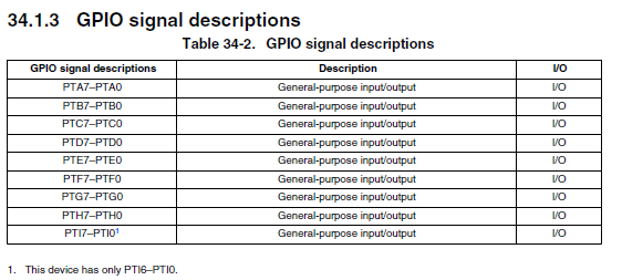
GPIO signal Descriptions is described in following table, page 678
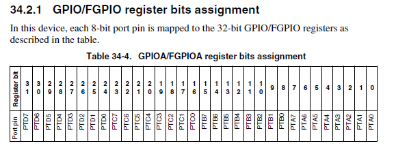
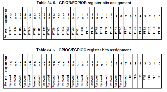
If you mean GPIO/FGPIO register bits assignment, please go to Reference Manual for KE06, page 679
http://cache.freescale.com/files/microcontrollers/doc/ref_manual/MKE06P80M48SF0RM.pdf?fasp=1
I hope the information help you,
Best Regards,
Iva
Hello fan xy,
please, try it by this way:
GPIOB_PDDR |= GPIO_PDDR_PDD(1<<1); //PTB1 as output
GPIOB_PCOR |= GPIO_PCOR_PTCO(1<<1); //set PTB1 to log0
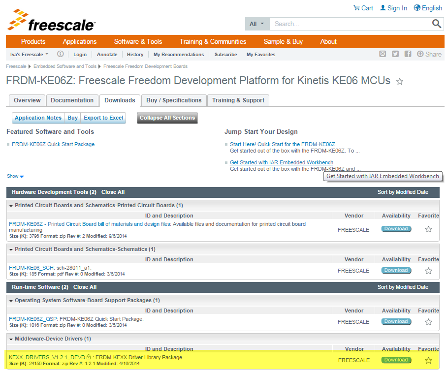
You can also invite drivers and examples (for gpio), which can help you.
Freescale Freedom Development Platform for Ki|Freescale
I hope it helps you,
Best Regards,
Iva
Hi,
Thank for your reply !
Maybe i did not say clearly.
I know this two instruction is to configure the gpio direction and data. While i want to know how to configure the pin to GPIO fuction.
For example "PTB1" pin, this pin can be used to "UART0_TX" "ADC0_SE5" or "GPIO" function,
and how to configure it to "GPIO" or "UARTO_TX" .
Thank
Well, now we're showing my general lack of familiarity with the KE06 in particular. But downloading the manual MKE06P80M48SF0RM.pdf, section 10.2.1 details which 'alternate zero thru seven' will select for a pin, the first paragraph of which has this statement:
The Port Control Module is responsible for selecting which ALT functionality is available on each pin.
I assumed that was TRUE, and hence my prior suggestions.
That being said, I SEE YOUR POINT -- chapter 11, Port Control, makes NO mention of such Port Control Registers (as I use in the 'K' family).
It appears that for this family SOME control is REALLY in the SIM_PINSELx registers (12.2.4&5). But I'm afraid I have to agree with you on this one! It is NOT obvious how this works. In the table on page 141, PTB1 can serve as PTB1, KB0_P9, UART0_TX, and ADC0_SE5 (default). So I can see how UART0PS can move UART0 'away' from PortB (although i DON'T see how you keep UART0 from taking ANY I/O pins, maybe if it is not 'clock enabled'?), but that can't POSSIBLY be the whole story!
SO, I have to 'bow out' on being ANY HELP AT ALL (SORRY!), and we need to find someone more familiar with KE to help!
The pins usually default to GPIO functionality. In the example you give where you have UART and ADC pins shared with GPIO, turning on the UART transmit enable or receive enable bits then use the pins that are assigned for that purpose. In the case of the ADC, turning on the ADC channel enable bits assign those pins to the ADC. I'm not sure who wins if you have more than one function turned on, but having experienced the ADC taking control of a pin used for a SPI clock, all I can say is watch out for conflicts with pin functions.
Do NOT |= to PCOR. Read always returns zero, so read-modify-write (to 'or in') is a waste of code&time.
But more to the apparent question, pin function is configured in the pin-mux control, so Port Control needs to select GPIO function, generally Alternative #1:
PORTB_PCR1 = PORT_PCR_MUX(0x1); //Select PTB1 as GPIO, might also add any OTHER configuration options for this pin!
You choose the function on the pin. You cannot have more functions in the same time.
BR,
Iva
If you want to read data, you must read PDIR (Port Data Input Register).
Please, see p. 683
http://cache.freescale.com/files/microcontrollers/doc/ref_manual/MKE06P80M48SF0RM.pdf?fasp=1
BR,
Iva


