- Forums
- Product Forums
- General Purpose MicrocontrollersGeneral Purpose Microcontrollers
- i.MX Forumsi.MX Forums
- QorIQ Processing PlatformsQorIQ Processing Platforms
- Identification and SecurityIdentification and Security
- Power ManagementPower Management
- Wireless ConnectivityWireless Connectivity
- RFID / NFCRFID / NFC
- Advanced AnalogAdvanced Analog
- MCX Microcontrollers
- S32G
- S32K
- S32V
- MPC5xxx
- Other NXP Products
- S12 / MagniV Microcontrollers
- Powertrain and Electrification Analog Drivers
- Sensors
- Vybrid Processors
- Digital Signal Controllers
- 8-bit Microcontrollers
- ColdFire/68K Microcontrollers and Processors
- PowerQUICC Processors
- OSBDM and TBDML
- S32M
- S32Z/E
-
- Solution Forums
- Software Forums
- MCUXpresso Software and ToolsMCUXpresso Software and Tools
- CodeWarriorCodeWarrior
- MQX Software SolutionsMQX Software Solutions
- Model-Based Design Toolbox (MBDT)Model-Based Design Toolbox (MBDT)
- FreeMASTER
- eIQ Machine Learning Software
- Embedded Software and Tools Clinic
- S32 SDK
- S32 Design Studio
- GUI Guider
- Zephyr Project
- Voice Technology
- Application Software Packs
- Secure Provisioning SDK (SPSDK)
- Processor Expert Software
- Generative AI & LLMs
-
- Topics
- Mobile Robotics - Drones and RoversMobile Robotics - Drones and Rovers
- NXP Training ContentNXP Training Content
- University ProgramsUniversity Programs
- Rapid IoT
- NXP Designs
- SafeAssure-Community
- OSS Security & Maintenance
- Using Our Community
-
- Cloud Lab Forums
-
- Knowledge Bases
- ARM Microcontrollers
- i.MX Processors
- Identification and Security
- Model-Based Design Toolbox (MBDT)
- QorIQ Processing Platforms
- S32 Automotive Processing Platform
- Wireless Connectivity
- CodeWarrior
- MCUXpresso Suite of Software and Tools
- MQX Software Solutions
- RFID / NFC
- Advanced Analog
-
- NXP Tech Blogs
- Home
- :
- General Purpose Microcontrollers
- :
- Kinetis Microcontrollers
- :
- Re: Verify error at address 0x0000040D, target byte: 0x3D, byte in file: 0x3F
Verify error at address 0x0000040D, target byte: 0x3D, byte in file: 0x3F
- Subscribe to RSS Feed
- Mark Topic as New
- Mark Topic as Read
- Float this Topic for Current User
- Bookmark
- Subscribe
- Mute
- Printer Friendly Page
Verify error at address 0x0000040D, target byte: 0x3D, byte in file: 0x3F
- Mark as New
- Bookmark
- Subscribe
- Mute
- Subscribe to RSS Feed
- Permalink
- Report Inappropriate Content
Hi, I am working on the MKL27Z256VFM4 MCU and I am using IAR Embedded Workbench.
My project compiled successfully, but I received an error during the download to the target.
The warning is "Verify error at address 0x0000040D, target byte: 0x3D, byte in file: 0x3F"
Is any idea what is the problem about this? how to fix it? Will it cause any error in my program?
In addition, my project is working properly except two GPIO pins are not responding. Is this related to the above error?
or I configure my pins incorrectly? I have attached the pin_mux.c file below. Please advise.
void BOARD_InitPins(void)
{
CLOCK_EnableClock(kCLOCK_PortA);
PORT_SetPinMux(PORTA, 1U, kPORT_MuxAlt2);
PORT_SetPinMux(PORTA, 2U, kPORT_MuxAlt2);
PORT_SetPinMux(PORTA, 4U, kPORT_MuxAsGpio); <<< This pin is not responding.
CLOCK_EnableClock(kCLOCK_PortB);
port_pin_config_t Bconfig = {0};
Bconfig.pullSelect = kPORT_PullUp;
Bconfig.mux = kPORT_MuxAsGpio;
PORT_SetPinConfig(PORTB, 0U, &Bconfig);
PORT_SetPinMux(PORTB, 1U, kPORT_PinDisabledOrAnalog);
CLOCK_EnableClock(kCLOCK_PortC);
port_pin_config_t Cconfig = {0};
Cconfig.pullSelect = kPORT_PullUp;
Cconfig.mux = kPORT_MuxAsGpio;
PORT_SetPinConfig(PORTC, 1U, &Cconfig);
PORT_SetPinConfig(PORTC, 3U, &Cconfig);
PORT_SetPinConfig(PORTC, 4U, &Cconfig);
PORT_SetPinConfig(PORTC, 5U, &Cconfig);
PORT_SetPinConfig(PORTC, 6U, &Cconfig);
PORT_SetPinConfig(PORTC, 7U, &Cconfig);
CLOCK_EnableClock(kCLOCK_PortD);
PORT_SetPinMux(PORTD, 4U, kPORT_MuxAsGpio);
PORT_SetPinMux(PORTD, 5U, kPORT_MuxAsGpio);
CLOCK_EnableClock(kCLOCK_PortE);
PORT_SetPinMux(PORTE, 0U, kPORT_MuxAlt4); <<< This pin is not responding.
PORT_SetPinMux(PORTE, 30U, kPORT_MuxAsGpio); <<< This pin is not responding.
}
I simply toggle high and low on these three pin, but they have no response at all.
Any idea? Please kindly advise. Greatly Appreciate!!!
Regards,
Gilbert
- Mark as New
- Bookmark
- Subscribe
- Mute
- Subscribe to RSS Feed
- Permalink
- Report Inappropriate Content
Hi Gilbert Liu,
Your problem is caused by you modify the flash configuration field, this is protected by the IAR IDE.
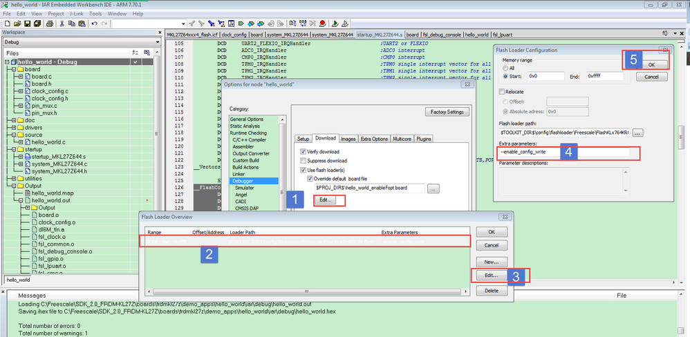
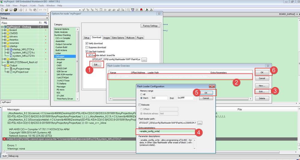
0x0000040D is the FOTP area, if you want you want to modify it, you need edit your .board to add the extra parameters:--enable_config_write
Just like this:
Before you download the code, please do a mass erase at first, then download the code again.
Your GPIO problem may caused by the code, please check whether your pin mux is correct.
PORT_SetPinMux(PORTE, 0U, kPORT_MuxAlt4); <<< This pin is not responding.
PORT_SetPinMux(PORTE, 30U, kPORT_MuxAsGpio); <<< This pin is not responding.
PTE0 ALT1 is the GPIO function, ALT4 is the RTC_CLKOUT function.
PTE30 is a special pin, when the VREF is enabled, PTE30 is the VREF_OUT pin.
Wish it helps you!
If you still have question, please contact me!
Have a great day,
Kerry
-----------------------------------------------------------------------------------------------------------------------
Note: If this post answers your question, please click the Correct Answer button. Thank you!
-----------------------------------------------------------------------------------------------------------------------
- Mark as New
- Bookmark
- Subscribe
- Mute
- Subscribe to RSS Feed
- Permalink
- Report Inappropriate Content
Hi Kerry,
Thanks for your recommendation. Unfortunately, still have the same problem.
For the download issue, I followed exactly what you told me, but the same error still exists.
FYI, I am working with the MKL27Z256VFM4, so the flash loader file is pointing to "FlashKLxx256KROM.flash".
I noticed you are using 64K from your image, any difference?
For the pin has no response, I have 3 pins have no response, which are PTA4, PTE0 and PTE30.
For the PTA4, I set it as GPIO correctly, but not working.
For the PTE0, I tried both GPIO or set it as the RTC_CLKOUT (as my code above), both settings are not working.
For the PTE30, I followed your recommendation, change the ADC0_SC2, REFSEL to 01, but still not working.
In addition, I am using "startup_MKL27Z4.s", "system_MKL27Z.c" and "system_MKL27Z4.h" in my startup folder.
I think this is correct for my MKL27Z256VFM4 MCU, is this correct?
Please advise in more detail. Thank you very much!
Regards,
Gilbert
- Mark as New
- Bookmark
- Subscribe
- Mute
- Subscribe to RSS Feed
- Permalink
- Report Inappropriate Content
Hi Gilbert,
Thank you for your more details!
Could you provide me your problem project? I need to help you to check it on my FRDM-KL43, because I don't have MKL27Z256VFM4 board on my side, but MKL27Z256VFM4 can be run in KL43, so you also can try the KSDK2.0-KL43 sample code on your side.
Yes, the picture I give you before is from FRDM-KL27, it is not directly for MKL27Z256VFM4, just give you a picture example.
Your start file and system file is correct, that is for MKL27Z256VFM4.
PTA4 is the special pin, it is the NMI pin, just modify the MUX can't set PTA4 to GPIO, if you want to use PTA4, you need to disable the NMI function in the flash configuration field, if your pin is enough to use, I don't suggest you use this pin as GPIO.
About the PTE0 and PTE30, please use this code:
PORTE->PCR[0] = PORT_PCR_MUX(1) | PORT_PCR_PE_MASK | PORT_PCR_PS_MASK;
PORTE->PCR[30] = PORT_PCR_MUX(1) | PORT_PCR_PE_MASK | PORT_PCR_PS_MASK;
GPIOE->PDDR |= (1<<30) |(1<<0);
GPIOE->PTOR |= (1<<30) |(1<<0);
GPIOE->PTOR |= (1<<30) |(1<<0);
GPIOE->PTOR |= (1<<30) |(1<<0);
GPIOE->PTOR |= (1<<30) |(1<<0);
I have test PTE0 and PTE30, it works on my side, please also check your hardware, did you connect it to other external component?
If you are still not ok, please send me your problem project, I would like to help you to check it.
Have a great day,
Kerry
-----------------------------------------------------------------------------------------------------------------------
Note: If this post answers your question, please click the Correct Answer button. Thank you!
-----------------------------------------------------------------------------------------------------------------------
- Mark as New
- Bookmark
- Subscribe
- Mute
- Subscribe to RSS Feed
- Permalink
- Report Inappropriate Content
Hi Kerry,
Please see my attached project.
By add the PDDR line, both the PTE0 and PTE30 work fine now.
In fact, I never touch the FOPT flash loader section before, but I still have the "Verify error at address 0x0000040D, target byte: 0x3D, byte in file: 0x3F " error.
Until now, I need to configure the PTA4 pin as a GPIO, unfortunately I used up all the pin, there is no pin left now.
So please advise the detail how to disable the NMI function on the PTA4 pin.
Furthermore, I would like to know if there is any affect if I disable the NMI, for instance, will this cause any problem with my existing interrupt in the project? Please advise in detail.
Thank you!
Regards,
Gilbert
- Mark as New
- Bookmark
- Subscribe
- Mute
- Subscribe to RSS Feed
- Permalink
- Report Inappropriate Content
Hi Gilbert,
The project you give missed a lot of source file, so the project have a lot of build errors on my side.
1. Just as what I have told you, your problem is not enable the flash configuration filed in the IAR, this problem is very very important!
Your problem is caused by you modify the flash configuration field, this is protected by the IAR IDE.
0x0000040D is the FOTP area, if you want you want to modify it, you need edit your .board to add the extra parameters:--enable_config_write
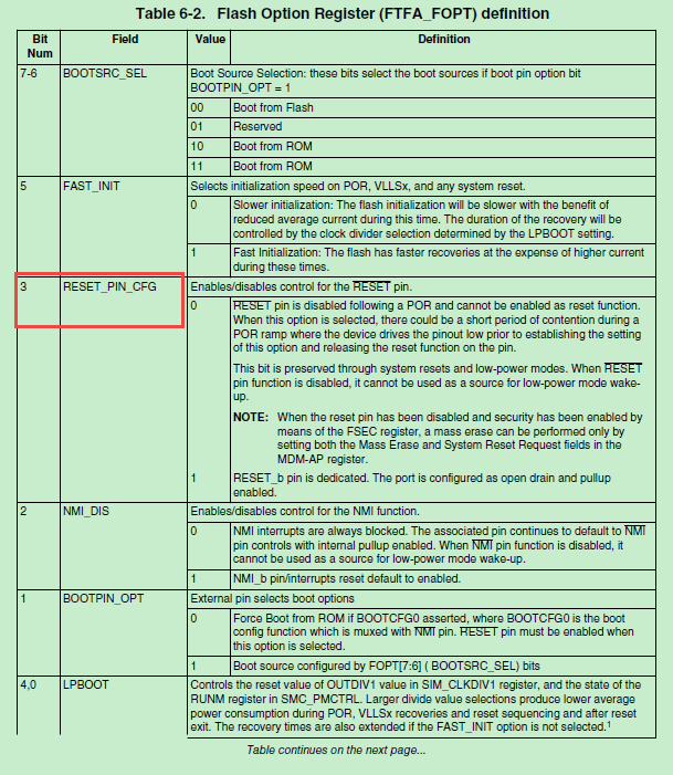
2. Your problem is report the 0X40D data, but what the function in the flash configuration filed 0x40d? Please read the reference manual:
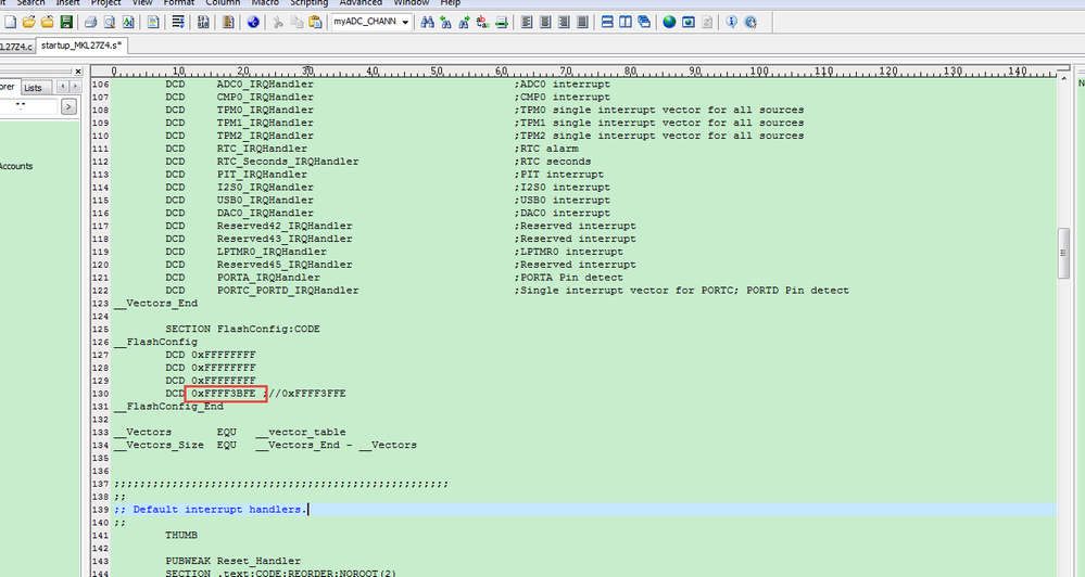
So, this area also can disable the NMI function, please modify your 0X40D data to 0X3B.
Open "startup_MKL27Z4.s" file, change line 130 to 0xFFFF3BFE
After the above 2 steps, then build again, download the code to your board, then PTA4 NMI function will be disabled, you can use it as the GPIO, it doen't matter.
Wish it helps you!
If you still have question, please contact me!
Have a great day,
Kerry
-----------------------------------------------------------------------------------------------------------------------
Note: If this post answers your question, please click the Correct Answer button. Thank you!
-----------------------------------------------------------------------------------------------------------------------
- Mark as New
- Bookmark
- Subscribe
- Mute
- Subscribe to RSS Feed
- Permalink
- Report Inappropriate Content
Hi Kerry,
Thank you very much for your help, all my previous concerns have been solved.
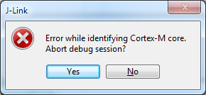
In addition, I have a problem with first program to new MCU now, refer to our earlier conversation, you advised me to erase the memory before the program. But I encounter some problem when I program the new MCU, which one of the problem as the following:
I also have my IAR is "Not Responding" when I program the MCU sometimes.
Is this due to the FOPT area has been modified?
Please advise the best way to program the my MCU to avoid all these problems.
Thank you again!
Greatly appreciate your great help!
Regards,
Gilbert
- Mark as New
- Bookmark
- Subscribe
- Mute
- Subscribe to RSS Feed
- Permalink
- Report Inappropriate Content
Hi Gilbert,
Did you design the board by yourself?
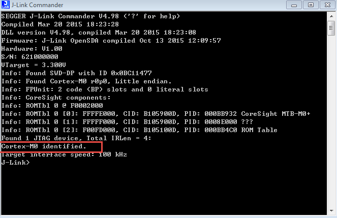
When the picture you send me happens, you can use the JLINK command to check it, whether it can find the Core or not?
About the hardware, please check these points:
Reset Pin: need external 4.7k to 10k pull up resistor, and 0.1uf capacitor to ground.
NMI pin: need external 4.7K to 10K pull up resistor.
The debugger wire can't be too long between the board and your debugger.
Wish it helps you!
Have a great day,
Kerry
-----------------------------------------------------------------------------------------------------------------------
Note: If this post answers your question, please click the Correct Answer button. Thank you!
-----------------------------------------------------------------------------------------------------------------------
- Mark as New
- Bookmark
- Subscribe
- Mute
- Subscribe to RSS Feed
- Permalink
- Report Inappropriate Content
Hi Kerry,
Yes, I am working my my own board.
Please advise the information how to use the JLink command to check. Thanks.
Yes, I have all the correct bypass cap and resistors on those pins.
Anyway, I copied the debug log and attached below for your information.
_____________________________________________________________________________________
Wed Nov 09, 2016 11:07:43: Device "MKL27Z256XXX4" selected.
Wed Nov 09, 2016 11:07:43: DLL version: V4.98e, compiled May 5 2015 11:00:52
Wed Nov 09, 2016 11:07:43: Firmware: J-Link V9 compiled Apr 22 2016 11:47:06
Wed Nov 09, 2016 11:07:43: Selecting SWD as current target interface.
Wed Nov 09, 2016 11:07:43: JTAG speed is initially set to: 32 kHz
Wed Nov 09, 2016 11:07:43: Found SWD-DP with ID 0x0BC11477
Wed Nov 09, 2016 11:07:43: Found SWD-DP with ID 0x0BC11477
Wed Nov 09, 2016 11:07:43: Found Cortex-M0 r0p1, Little endian.
Wed Nov 09, 2016 11:07:43: FPUnit: 2 code (BP) slots and 0 literal slots
Wed Nov 09, 2016 11:07:43: CoreSight components:
Wed Nov 09, 2016 11:07:43: ROMTbl 0 @ F0002000
Wed Nov 09, 2016 11:07:43: ROMTbl 0 [0]: FFFFE000, CID: B105900D, PID: 001BB932 MTB-M0+
Wed Nov 09, 2016 11:07:43: ROMTbl 0 [1]: FFFFF000, CID: B105900D, PID: 0008E000 MTBDWT
Wed Nov 09, 2016 11:07:43: ROMTbl 0 [2]: F00FD000, CID: B105100D, PID: 000BB4C0 ROM Table
Wed Nov 09, 2016 11:07:43: ROMTbl 1 @ E00FF000
Wed Nov 09, 2016 11:07:43: ROMTbl 1 [0]: FFF0F000, CID: B105E00D, PID: 000BB008 SCS
Wed Nov 09, 2016 11:07:43: ROMTbl 1 [1]: FFF02000, CID: B105E00D, PID: 000BB00A DWT
Wed Nov 09, 2016 11:07:43: ROMTbl 1 [2]: FFF03000, CID: B105E00D, PID: 000BB00B FPB
Wed Nov 09, 2016 11:07:44: SYSRESETREQ has confused core. Trying to reconnect and use VECTRESET.
Wed Nov 09, 2016 11:07:44: Found SWD-DP with ID 0x0BC11477
Wed Nov 09, 2016 11:07:44: Warning: Failed to reset CPU. VECTRESET has confused core.
Wed Nov 09, 2016 11:07:44: Warning: RESET (pin 15) high, but should be low. Please check target hardware.
Wed Nov 09, 2016 11:07:44: Warning: CPU did not halt after reset.
Wed Nov 09, 2016 11:07:44: Warning: CPU could not be halted
Wed Nov 09, 2016 11:07:44: Core did not halt after reset, trying to disable WDT.
Wed Nov 09, 2016 11:07:44: Warning: RESET (pin 15) high, but should be low. Please check target hardware.
Wed Nov 09, 2016 11:07:45: Warning: CPU did not halt after reset.
Wed Nov 09, 2016 11:07:45: Warning: CPU could not be halted
Wed Nov 09, 2016 11:07:45: Warning: S_RESET_ST not cleared
Wed Nov 09, 2016 11:07:45: Warning: RESET (pin 15) high, but should be low. Please check target hardware.
Wed Nov 09, 2016 11:07:45: Found SWD-DP with ID 0x0BC11477
Wed Nov 09, 2016 11:07:45: SYSRESETREQ has confused core. Trying to reconnect and use VECTRESET.
Wed Nov 09, 2016 11:07:45: Found SWD-DP with ID 0x0BC11477
Wed Nov 09, 2016 11:07:45: Warning: Failed to reset CPU. VECTRESET has confused core.
Wed Nov 09, 2016 11:07:45: Warning: RESET (pin 15) high, but should be low. Please check target hardware.
Wed Nov 09, 2016 11:07:45: Warning: CPU did not halt after reset.
Wed Nov 09, 2016 11:07:46: Warning: CPU could not be halted
Wed Nov 09, 2016 11:07:46: Core did not halt after reset, trying to disable WDT.
Wed Nov 09, 2016 11:07:46: Warning: RESET (pin 15) high, but should be low. Please check target hardware.
Wed Nov 09, 2016 11:07:46: Warning: CPU did not halt after reset.
Wed Nov 09, 2016 11:07:46: Warning: CPU could not be halted
Wed Nov 09, 2016 11:07:46: Warning: S_RESET_ST not cleared
Wed Nov 09, 2016 11:07:51: Fatal error: Error while identifying Cortex-M core. Session aborted!
Wed Nov 09, 2016 11:07:51: Unloaded macro file: C:\Program Files (x86)\IAR Systems\Embedded Workbench 7.2\arm\config\flashloader\Freescale\FlashKLxx.mac
_____________________________________________________________________________________
I have no idea why it warns the RESET (pin 15), but on my MCU MKL27Z256VFM4 the reset is PTA20 (pin 19).
Please advise.
Again, thanks a lot and greatly appreciate your help!
Regards,
Gilbert
- Mark as New
- Bookmark
- Subscribe
- Mute
- Subscribe to RSS Feed
- Permalink
- Report Inappropriate Content
Hi Gilbert,
Use the JLINK to connect your board, then open JLINK Commander window which you can find in your JLINK driver install path.
This means you can find the core, if you can't find the core in your new board in the first time, you need to check your hardware.
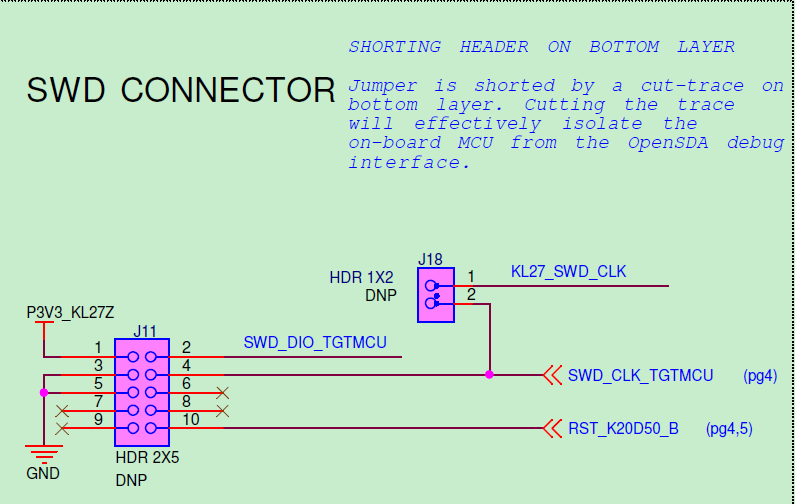
About the reset, did you connect the reset pin to the SWD interface?
Please refer to the FRDM-KL27 to design the SWD interface:
SWD_DIO need add 10K pull up resistor.
Reset need add 4.7k to 10K pullup resistor, and connect a 0.1uf capacitor to ground.
NMI need add 4.7K to 10K pullup resistor.
Please also check you hardware.
Wish it helps you.
Have a great day,
Kerry
-----------------------------------------------------------------------------------------------------------------------
Note: If this post answers your question, please click the Correct Answer button. Thank you!
-----------------------------------------------------------------------------------------------------------------------
- Mark as New
- Bookmark
- Subscribe
- Mute
- Subscribe to RSS Feed
- Permalink
- Report Inappropriate Content
Hi Kerry,
Sorry for the late reply because I spent sometimes to make sure everything is working properly.
Anyway, I followed all your recommendation to check my board and found there is a pin shorted on my programming header. everything works fine after this fix.
Thank you very much for your patience and advise.
I greatly appreciate your help.
Regards,
Gilbert
