- Forums
- Product Forums
- General Purpose MicrocontrollersGeneral Purpose Microcontrollers
- i.MX Forumsi.MX Forums
- QorIQ Processing PlatformsQorIQ Processing Platforms
- Identification and SecurityIdentification and Security
- Power ManagementPower Management
- Wireless ConnectivityWireless Connectivity
- RFID / NFCRFID / NFC
- Advanced AnalogAdvanced Analog
- MCX Microcontrollers
- S32G
- S32K
- S32V
- MPC5xxx
- Other NXP Products
- S12 / MagniV Microcontrollers
- Powertrain and Electrification Analog Drivers
- Sensors
- Vybrid Processors
- Digital Signal Controllers
- 8-bit Microcontrollers
- ColdFire/68K Microcontrollers and Processors
- PowerQUICC Processors
- OSBDM and TBDML
- S32M
- S32Z/E
-
- Solution Forums
- Software Forums
- MCUXpresso Software and ToolsMCUXpresso Software and Tools
- CodeWarriorCodeWarrior
- MQX Software SolutionsMQX Software Solutions
- Model-Based Design Toolbox (MBDT)Model-Based Design Toolbox (MBDT)
- FreeMASTER
- eIQ Machine Learning Software
- Embedded Software and Tools Clinic
- S32 SDK
- S32 Design Studio
- GUI Guider
- Zephyr Project
- Voice Technology
- Application Software Packs
- Secure Provisioning SDK (SPSDK)
- Processor Expert Software
- Generative AI & LLMs
-
- Topics
- Mobile Robotics - Drones and RoversMobile Robotics - Drones and Rovers
- NXP Training ContentNXP Training Content
- University ProgramsUniversity Programs
- Rapid IoT
- NXP Designs
- SafeAssure-Community
- OSS Security & Maintenance
- Using Our Community
-
- Cloud Lab Forums
-
- Knowledge Bases
- ARM Microcontrollers
- i.MX Processors
- Identification and Security
- Model-Based Design Toolbox (MBDT)
- QorIQ Processing Platforms
- S32 Automotive Processing Platform
- Wireless Connectivity
- CodeWarrior
- MCUXpresso Suite of Software and Tools
- MQX Software Solutions
- RFID / NFC
- Advanced Analog
-
- NXP Tech Blogs
- Home
- :
- 通用微控制器
- :
- Kinetis微控制器
- :
- Re: MK66F custom board + LPC LINK2 JTAG problems
MK66F custom board + LPC LINK2 JTAG problems
MK66F custom board + LPC LINK2 JTAG problems
Hello,
I am working on a project that needed a custom board using the kinetis mk66 microcontroller.
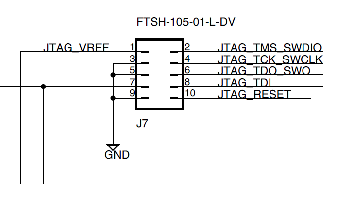
I have no space for a sda chip on the board so i am using the LPC LINK2 (J7) as the debugger using MCUXpresso IDE.
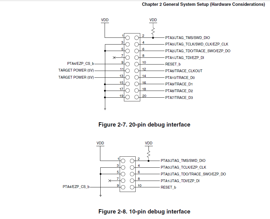
I have designed the jtag using the recommendations as per section 65.2 External signal description(page 2225/2247) and 10.3 Debug Port Pin Descriptions ( page 179/2247) with no external resistors attached.
The debugger soft loaded its firmware(CMSIS-DAP) and is seen by the MCUXpresso IDE.
I am powering my custom board from an external power supply so JP2 si off.
As this is my first design i have unfortunately not used the Reset_b pin and it is floating.
The first time i tried to flash the mk66,using the gui flash tool, i unknowingly performed a MASS ERASE and it looks like the reset mcu box is also ticked. Se i did a MASS ERASE + RESET and i have read it might be bricked ?
I will post pictures of the error i recieve .
Also, the unlock from the GUI Flash Tool does not work.
I have also measured the voltage between the pins and gnd to verify that the signals are pulled high/low as per the 65.2 External signal description. I have tried pulling the JTAG_TRST_b pin high by 10k resistor. I tried pulling TDO(because it has no internal pull) low and high and nothing happened.
I have imported the mk66f sdk and imported a project in the workspace.
I have also tried changing the launch configuration from SWD to JTAG in Debug Connection and changing the Vector catch and still nothing.
I keep getting the same error: Wire ACK fault in DAP access.
Is there anything i might do at this point ? Could i load the j-link firmware in the LPC Link2 and use the j-link debugger command window to issue some unlock or something ?
I will post screen shots .
After adding the 2 NMI_b and Reset_b pins and pulling-up the TMS pin I still cannot acces my microcontroller using the jtag-LpcLink2 and MCUXpresso IDE.
Things that are different in my JTAG hardware connections are :
As i am using the J7 of the lpc link2 i have routed my pins so that they match this schematic and not what you suggested.
Also i don't think i should route the PTA4/EZP_cs to pin9 of the 10 pin connector because the lpc_link2 connects that pin to GND so it would force my controller to enter EZPort mode, right ?
Any thoughts ?
Hi Bogdan Nica
PTA4 is the very special pin, it is the NMI pin, so you need to add external 4.7K to 10K pull up in the pin.
If you don't want to use the EZport, you totally don't need to connect PTA4 in your JTAG interface.
From my opinion, you also can use the SWD interface, this interface just need 5 pins:
VDD, VSS, SWD_CLK, SWD_DIO, RESET
SWD_DIO need external 10K pull up resistor, RESET_b need external 4.7K to 10K pull up resistor and 0.1uf capacitor to ground.
Then, you can use the JLINK firmware in the LPC-LINK2, then use the JLINK commander to connect the chip, if you can find the ARM core, it means your hardware is OK, if you can't find the ARM core, it means your hardware still have problems.
Wish it helps you!
If you still have question about it, please kindly let me know.
Have a great day,
Kerry
-------------------------------------------------------------------------------
Note:
- If this post answers your question, please click the "Mark Correct" button. Thank you!
- We are following threads for 7 weeks after the last post, later replies are ignored
Please open a new thread and refer to the closed one, if you have a related question at a later point in time.
-------------------------------------------------------------------------------
Hello and thank you for the help.
I swapped the mico with a fresh one and it worked.
I ended up not using any passive components on the NMI nor the RESET pins and simpli left them not connected on my pcb . I did use the pull up on the Jtag_tms pin .
My board works and I tested the hello_world and it printed in the IDE console.
It simply looks like the controller was bricked and now seems to be ok.
I do have another question though.
I am using the mk66 sdk and cannot set a pin to high using the PinWrite function.
Does it have anything to do with the fact that the sdk is using a 12MHz clock while I am using a 16MHz one ? (I checked my 16MHz clock on the oscilloscope and it is fine ).
Hi Bogdan Nica,
It's very good to hear you make it works on your side.
About your new question, do you want to use one pin as the GPIO and output to high?
If yes, you can refer to the SDK led blinky code.
If you still have problems, could you please create a new question post, then you can @kerry zhou, then I will help you to check the details in your new question post, thank you!
Have a great day,
Kerry
-------------------------------------------------------------------------------
Note:
- If this post answers your question, please click the "Mark Correct" button. Thank you!
- We are following threads for 7 weeks after the last post, later replies are ignored
Please open a new thread and refer to the closed one, if you have a related question at a later point in time.
-------------------------------------------------------------------------------
Hi Bogdan Nica ,
You CAN'T leave RESET pin floating!
Reset pin should have external 4.7K to 10K pull up, and 0.1uf capacitor to ground.
NMI pin need external 4.7K to 10K pull up resistor.
SWD interface need these pin: VDD, GND, RESET, SWD_DIO, SWD_CLK.
SWD_DIO need to add external 10K pull up resistor.
You must make sure your hardware is OK, otherwise it will have problem.
I suggest you use the LPC-LINK2 with the jlink firmware, then use the JILNK commander to connect your board, if it can find the ARM core, it means your hardware still have problem, you need to check the hardware at first.
So, please use the JLINK commander to connect your board at first, then give me the result.
Wish it helps you!
If you still have question about it, please kindly let me know.
Have a great day,
Kerry
-------------------------------------------------------------------------------
Note:
- If this post answers your question, please click the "Mark Correct" button. Thank you!
- We are following threads for 7 weeks after the last post, later replies are ignored
Please open a new thread and refer to the closed one, if you have a related question at a later point in time.
-------------------------------------------------------------------------------
Cool,
Thx for the reply.
I will be doing some improvements on my pcb and i have a couple more questions :
1. I will be using JTAG so what pull should i use for JTAG_TCLK , JTAG_TDI, JTAG_TDO, JTAG_TMS(pull-up) ,JTAG_
TRST_b ? And why isn't the internal pull enough ? Are the values of the pull resistors to low ?
2. Also , i have seen various comments about how to wire together VREFL and VSSA pins together.I will not use any analog supply nor any ADC functionality si is it ok if i just wire VREFL and VSSA pins together and ground them or should i add anything else ?
Hi Bogdan Nica,
Answer your two questions:
1. About the external pull up
You can refer to this document:
https://cache.freescale.com/files/32bit/doc/quick_ref_guide/KQRUG.pdf
Internal pull up is weak, so to work stably, it's better to add the external pull up resistor.
2. To the unused power pin
It's better to connect it to the expected power.
So, it's better to connect VDDA VREFH to VDD, VSSA VREFL to GND.
Wish it helps you!
If you still have question about it, please kindly let me know.
Have a great day,
Kerry
-------------------------------------------------------------------------------
Note:
- If this post answers your question, please click the "Mark Correct" button. Thank you!
- We are following threads for 7 weeks after the last post, later replies are ignored
Please open a new thread and refer to the closed one, if you have a related question at a later point in time.
-------------------------------------------------------------------------------
I have currently connected VSSA and VREFL to GND as this is what i have found on FRDM-K66F schematic.
I have also connected VDDA and VREFL to VDD .
Will this not work out ?
Won't i get an internal short circuit if i take your advice and connect VSSA VREFL to VDD ?
Hi Bogdan Nica,
So sorry for my misleading in the last reply, it's totally mistyping.
it's better to connect VDDA VREFH to VDD, VSSA VREFL to GND.
So, you connect VSSA and VREFL to GND, it is correct.
You can refer to the FRDM-K66 schematic.
Have a great day,
Kerry
-------------------------------------------------------------------------------
Note:
- If this post answers your question, please click the "Mark Correct" button. Thank you!
- We are following threads for 7 weeks after the last post, later replies are ignored
Please open a new thread and refer to the closed one, if you have a related question at a later point in time.
-------------------------------------------------------------------------------


