- Forums
- Product Forums
- General Purpose MicrocontrollersGeneral Purpose Microcontrollers
- i.MX Forumsi.MX Forums
- QorIQ Processing PlatformsQorIQ Processing Platforms
- Identification and SecurityIdentification and Security
- Power ManagementPower Management
- Wireless ConnectivityWireless Connectivity
- RFID / NFCRFID / NFC
- Advanced AnalogAdvanced Analog
- MCX Microcontrollers
- S32G
- S32K
- S32V
- MPC5xxx
- Other NXP Products
- S12 / MagniV Microcontrollers
- Powertrain and Electrification Analog Drivers
- Sensors
- Vybrid Processors
- Digital Signal Controllers
- 8-bit Microcontrollers
- ColdFire/68K Microcontrollers and Processors
- PowerQUICC Processors
- OSBDM and TBDML
- S32M
- S32Z/E
-
- Solution Forums
- Software Forums
- MCUXpresso Software and ToolsMCUXpresso Software and Tools
- CodeWarriorCodeWarrior
- MQX Software SolutionsMQX Software Solutions
- Model-Based Design Toolbox (MBDT)Model-Based Design Toolbox (MBDT)
- FreeMASTER
- eIQ Machine Learning Software
- Embedded Software and Tools Clinic
- S32 SDK
- S32 Design Studio
- GUI Guider
- Zephyr Project
- Voice Technology
- Application Software Packs
- Secure Provisioning SDK (SPSDK)
- Processor Expert Software
- Generative AI & LLMs
-
- Topics
- Mobile Robotics - Drones and RoversMobile Robotics - Drones and Rovers
- NXP Training ContentNXP Training Content
- University ProgramsUniversity Programs
- Rapid IoT
- NXP Designs
- SafeAssure-Community
- OSS Security & Maintenance
- Using Our Community
-
- Cloud Lab Forums
-
- Knowledge Bases
- ARM Microcontrollers
- i.MX Processors
- Identification and Security
- Model-Based Design Toolbox (MBDT)
- QorIQ Processing Platforms
- S32 Automotive Processing Platform
- Wireless Connectivity
- CodeWarrior
- MCUXpresso Suite of Software and Tools
- MQX Software Solutions
- RFID / NFC
- Advanced Analog
-
- NXP Tech Blogs
- Home
- :
- General Purpose Microcontrollers
- :
- Kinetis Microcontrollers
- :
- Re: K66 USB regulator
K66 USB regulator
- Subscribe to RSS Feed
- Mark Topic as New
- Mark Topic as Read
- Float this Topic for Current User
- Bookmark
- Subscribe
- Mute
- Printer Friendly Page
K66 USB regulator
- Mark as New
- Bookmark
- Subscribe
- Mute
- Subscribe to RSS Feed
- Permalink
- Report Inappropriate Content
Hi All,
I'm doing a new hardware design with the K66, and it is to use high speed USB1 peripheral in device mode only. There is no requirement for bus or battery power. My question concerns the USB regulator. My preference would be to not use the USB reg at all and instead power the USB peripherals from the board's efficient 3.3V supply. Furthermore, from a layout standpoint it would be nice to not have to provide the 2.2uF cap on VREG_OUT.
If this regulator is not needed, but USB is required, would it be acceptable to simply tie all of VREG_IN0, VREG_IN1, and VREG_OUT to VDD ?
George
- Mark as New
- Bookmark
- Subscribe
- Mute
- Subscribe to RSS Feed
- Permalink
- Report Inappropriate Content
George,
What did you end up doing here? I have the same question as you - and Isaac didn't really answer it.
Isaac is right that the the USB phy is powered by VREG_OUT. But the datasheet indicates that VREG_OUT can operate the phy down to 3.0V, and dropout is < 300mV, so it should be ok to power the linear input (VREG_IN) via 3.3V instead of 5V, so I disagree with Isaac on that detail. Actually another spot in the datasheet indicates that for VREG_INx: "Operation range is 2.7 V to 5.5 V; tolerance voltage is up to 6 V"
It would seem a step better to do what you suggested, tie VREG_IN0, VREG_IN1, and VREG_OUT to +3.3V, not using the regulator at all, and eliminate a capacitor requirement.
Did you try this? I might try it... But I would like a "real" answer from NXP.
Thanks!
Jason
- Mark as New
- Bookmark
- Subscribe
- Mute
- Subscribe to RSS Feed
- Permalink
- Report Inappropriate Content
Hi Jason,
Sorry that I am just now seeing this note. I ended up not trying my idea so as not take any risk. However, I think that it is likely to work and might pursue it if I had some motivation.
Geo.
- Mark as New
- Bookmark
- Subscribe
- Mute
- Subscribe to RSS Feed
- Permalink
- Report Inappropriate Content
Hi Jason, I have the same question since I'm using the USB DM/DP pins but don't need the USB regulator. I know I'm asking a question of your question, but did you ever find an answer yourself on this?
- Mark as New
- Bookmark
- Subscribe
- Mute
- Subscribe to RSS Feed
- Permalink
- Report Inappropriate Content
Hello George,
I omitted one thing, this consideration applies only when USB is not being used, in your case, although USB will be configured to work as Device, you need to use internal USB Regulator.
Indeed USB HS uses the internal USB PHY and during PHY initialization, it requires that VREGIN0 and VREGIN1 are connected to 5V input.
VREGOUT output is used to power USB-FS and USB-HS modules so you need to use this USB regulator.
Hope this helps! And sorry for the confusion!
Regards,
Isaac
- Mark as New
- Bookmark
- Subscribe
- Mute
- Subscribe to RSS Feed
- Permalink
- Report Inappropriate Content
Hello George,
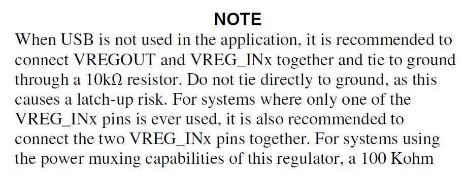
When USB Reg is not being used, it is recommended that VREG_OUT si connected to VREG_IN and both should be tied to GND by a 10 k resistor. This will prevent to increase current consumption on these pins.
Chapter 53 (USB Voltage Regulator) talks more about this.
Hope this helps!
regards,
Isaac
