- Forums
- Product Forums
- General Purpose MicrocontrollersGeneral Purpose Microcontrollers
- i.MX Forumsi.MX Forums
- QorIQ Processing PlatformsQorIQ Processing Platforms
- Identification and SecurityIdentification and Security
- Power ManagementPower Management
- Wireless ConnectivityWireless Connectivity
- RFID / NFCRFID / NFC
- Advanced AnalogAdvanced Analog
- MCX Microcontrollers
- S32G
- S32K
- S32V
- MPC5xxx
- Other NXP Products
- S12 / MagniV Microcontrollers
- Powertrain and Electrification Analog Drivers
- Sensors
- Vybrid Processors
- Digital Signal Controllers
- 8-bit Microcontrollers
- ColdFire/68K Microcontrollers and Processors
- PowerQUICC Processors
- OSBDM and TBDML
- S32M
- S32Z/E
-
- Solution Forums
- Software Forums
- MCUXpresso Software and ToolsMCUXpresso Software and Tools
- CodeWarriorCodeWarrior
- MQX Software SolutionsMQX Software Solutions
- Model-Based Design Toolbox (MBDT)Model-Based Design Toolbox (MBDT)
- FreeMASTER
- eIQ Machine Learning Software
- Embedded Software and Tools Clinic
- S32 SDK
- S32 Design Studio
- GUI Guider
- Zephyr Project
- Voice Technology
- Application Software Packs
- Secure Provisioning SDK (SPSDK)
- Processor Expert Software
- Generative AI & LLMs
-
- Topics
- Mobile Robotics - Drones and RoversMobile Robotics - Drones and Rovers
- NXP Training ContentNXP Training Content
- University ProgramsUniversity Programs
- Rapid IoT
- NXP Designs
- SafeAssure-Community
- OSS Security & Maintenance
- Using Our Community
-
- Cloud Lab Forums
-
- Knowledge Bases
- ARM Microcontrollers
- i.MX Processors
- Identification and Security
- Model-Based Design Toolbox (MBDT)
- QorIQ Processing Platforms
- S32 Automotive Processing Platform
- Wireless Connectivity
- CodeWarrior
- MCUXpresso Suite of Software and Tools
- MQX Software Solutions
- RFID / NFC
- Advanced Analog
-
- NXP Tech Blogs
- Home
- :
- General Purpose Microcontrollers
- :
- Kinetis Microcontrollers
- :
- DMA Destination Offset Confusion
DMA Destination Offset Confusion
- Subscribe to RSS Feed
- Mark Topic as New
- Mark Topic as Read
- Float this Topic for Current User
- Bookmark
- Subscribe
- Mute
- Printer Friendly Page
- Mark as New
- Bookmark
- Subscribe
- Mute
- Subscribe to RSS Feed
- Permalink
- Report Inappropriate Content
I am trying to implement DMA for receiving I2S channel 0 on a FRDM K22F. I got the I2S working and the I2S0_RDR0 register is updating with data; FIFO Request DMA is enabled. I am trying to store the data in an array 1024 long, each bin with 32 bits. That should be 4096 bytes. Here is my code
SIM_SCGC6 |= 0x2; //DMAMUX Module Turn On
SIM_SCGC7 |= 0x2; //DMA Module Turn On
DMAMUX_CHCFG0 = 0x8C; //I2S Source: Slot 12 & Activate
DMA_TCD0_CSR &= 0xBF; //Inactive
NVIC_EnableIRQ(DMA0_IRQn); //Enable IRQ DMA Channel 0
DMA_CR = 0x80; //Enable Minor Looping
DMA_TCD0_SADDR = (uint32_t)&I2S0_RDR0; //Data Source
DMA_TCD0_DADDR = (uint32_t) BUFFER_A; //Destination
DMA_TCD0_SOFF = 0; //No Source Offset
DMA_TCD0_SLAST = 0; //Nothing Added to Source Address after Major Loop
DMA_TCD0_DLASTSGA = -4096; //Value Added to Destination Address after Major Loop
DMA_TCD0_DOFF = 4; //4 Byte Destination Offset
//DMA_TCD0_NBYTES_MLOFFYES = 0x40001004; //DMLOE Set, MLOFF = 4 bytes, NBYTES = 4
DMA_TCD0_NBYTES_MLNO = 4; //4 Bytes Transfered in each Minor Loop
DMA_TCD0_BITER_ELINKNO = 1024; //1024 Bins
DMA_TCD0_CITER_ELINKNO = 1024; //1024 Bins
DMA_TCD0_ATTR = 0x202; //32-Bit Transfer Size
DMA_TCD0_CSR = 0x2; //Interrupt Major Iteration
DMA_SERQ = 0x0; //Channel 0 Enable
DMA_TCD0_CSR |= 0x41; //Enable!
Right now my code is crashing, I am not sure why but I do think it has to do with the minor loop offset. What is the difference between DOFF and using the NBYTES_MLOFFYES offset?
Solved! Go to Solution.
- Mark as New
- Bookmark
- Subscribe
- Mute
- Subscribe to RSS Feed
- Permalink
- Report Inappropriate Content
The reason why the code crashes is that the compiler can't see the interrupt handler. I added a extern "c" void and now the code runs
extern "C" void DMA0_IRQHandler(){
    pc.printf("something\r\n");
    DMA_CINT = 0;
    //RX_CALL();
    //DMA_TCD0_DADDR = (uint32_t)BUFFER_A;
    return;
}
- Mark as New
- Bookmark
- Subscribe
- Mute
- Subscribe to RSS Feed
- Permalink
- Report Inappropriate Content
Unfortunately no. I have a while(1) loop in main which just reads the DADDR register to make sure it is updating correctly. Right now it seems to be going out of range which makes my code crash. If I use DOFF < 4 the register doesn't update.
40009010 --> 1fff0230
40009010 --> 1fff04dc
40009010 --> 1fff0788
40009010 --> 1fff0a38
40009010 --> 1fff0ce4
40009010 --> 1fff0f90
...CODE CRASHES
    SIM_SCGC6 |= 0x2;               //DMAMUX Module Turn On
    SIM_SCGC7 |= 0x2;               //DMA Module Turn On
    DMAMUX_CHCFG0 = 0x8C;           //I2S Source: Slot 12 & Activate

    DMA_TCD0_CSR &= 0xBF;           //Inactive
    NVIC_EnableIRQ(DMA0_IRQn);      //Enable IRQ DMA Channel 0
    //DMA_CR = 0x80;                  //Enable Minor Looping

    DMA_TCD0_SADDR = (uint32_t)&I2S0_RDR0;    //Data Source
    DMA_TCD0_DADDR = (uint32_t) BUFFER_A;     //Destination

    DMA_TCD0_SOFF = 0;              //No Source Offset
    DMA_TCD0_SLAST = 0;             //Nothing Added to Source Address after Major Loop
    DMA_TCD0_DLASTSGA = -4096;      //Value Added to Destination Address after Major Loop
    DMA_TCD0_DOFF = 4;              //4 Byte Destination Offset
    DMA_TCD0_NBYTES_MLNO = 4;       //4096 Bytes Transfered in Minor Loop
    DMA_TCD0_BITER_ELINKNO = 1024;  //1024 Bins
    DMA_TCD0_CITER_ELINKNO = 1024;  //1024 Bins
    DMA_TCD0_ATTR = 0x202;          //32-Bit Transfer Size
    DMA_TCD0_CSR = 0x2;             //Interrupt Major Iteration

    DMA_SERQ = 0x0;                 //Channel 0 Enable
    DMA_TCD0_CSR |= 0x41;           //Enable!
- Mark as New
- Bookmark
- Subscribe
- Mute
- Subscribe to RSS Feed
- Permalink
- Report Inappropriate Content
I think your 'SGA' address-adjustment (at the end-of-loop) needs to be 'one transfer' (4 bytes) less than the total, as the LAST transfer won't increment the value, or 4092.
- Mark as New
- Bookmark
- Subscribe
- Mute
- Subscribe to RSS Feed
- Permalink
- Report Inappropriate Content
Indeed, There are some mistakes
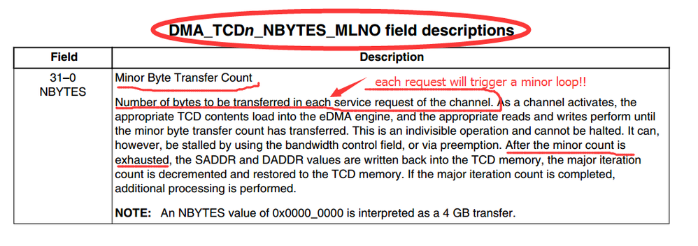
- the value in the register TCD Minor Byte Count (Minor Loop Disabled) (DMA_TCDn_NBYTES_MLNO) is Minor Byte Transfer Count,not the bytes Transfered in Major Loop
sorry, just now, i upload the wrong picture!!
- Mark as New
- Bookmark
- Subscribe
- Mute
- Subscribe to RSS Feed
- Permalink
- Report Inappropriate Content
I am aware of that. See my code.
However, MLNO is minor loop disabled, but it is indeed enabled in DMA_CR. NBYTES_MLOFFYES doesn't work either, I tried the commented out code but the MLOFF offset doesn't add to the DADDR register.
- Mark as New
- Bookmark
- Subscribe
- Mute
- Subscribe to RSS Feed
- Permalink
- Report Inappropriate Content
Hi Eduardo,
Is this issue solved? Please kindly let me know if you have any issue.
Have a great day,
Kan
-----------------------------------------------------------------------------------------------------------------------
Note: If this post answers your question, please click the Correct Answer button. Thank you!
-----------------------------------------------------------------------------------------------------------------------
- Mark as New
- Bookmark
- Subscribe
- Mute
- Subscribe to RSS Feed
- Permalink
- Report Inappropriate Content
AS to the difference between DOFF and using the NBYTES_MLOFFYES offset?
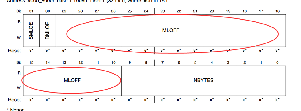
DOFF means the offset added to DADDR after every write to DADDR. But NBYTES_MLOFFYES offset means the offset added to DADDR after every minor loop if enabled.And one minor loop may include many times write.
you can see the example in the RMhttp://cache.freescale.com/files/microcontrollers/doc/ref_manual/K22P121M120SF7RM.pdf?fromsite=zh-Ha... P505
and you will get it.
- Mark as New
- Bookmark
- Subscribe
- Mute
- Subscribe to RSS Feed
- Permalink
- Report Inappropriate Content
oh, i get it
if you diable the minor loop remapping,the you shoud config DMA_TCD0_DOFF=4.
Or if you enable the minor loop remapping,then you should config the NBYTES_MLOFFYES
as showed the flowing two:
     SIM_SCGC6 |= 0x2;                      //DMAMUX Module Turn On
    SIM_SCGC7 |= 0x2;                       //DMA Module Turn On
    DMAMUX_CHCFG0 = 0x8C;           //I2S Source: Slot 12 & Activate

    DMA_TCD0_CSR &= 0xBF;            //Inactive
    NVIC_EnableIRQ(DMA0_IRQn);      //Enable IRQ DMA Channel 0
    //DMA_CR = 0x80;                         //Enable Minor Looping

    DMA_TCD0_SADDR = (uint32_t)&I2S0_RDR0;    //Data Source
    DMA_TCD0_DADDR = (uint32_t) BUFFER_A;      //Destination

    DMA_TCD0_SOFF = 0;                      //No Source Offset
    DMA_TCD0_SLAST = 0;                    //Nothing Added to Source Address after Major Loop
    DMA_TCD0_DLASTSGA = -4096;     //Value Added to Destination Address after Major Loop
    DMA_TCD0_DOFF = 4;                     //4 Byte Destination Offset

    //DMA_TCD0_NBYTES_MLOFFYES = 0x40001004; //DMLOE Set, MLOFF = 4 bytes, NBYTES = 4

    DMA_TCD0_NBYTES_MLNO = 4;         //4 Bytes Transfered in each Minor Loop
    DMA_TCD0_BITER_ELINKNO = 1024;   //1024 Bins
    DMA_TCD0_CITER_ELINKNO = 1024;  //1024 Bins
    DMA_TCD0_ATTR = 0x202;                //32-Bit Transfer Size
    DMA_TCD0_CSR = 0x2;                      //Interrupt Major Iteration

    DMA_SERQ = 0x0;                              //Channel 0 Enable
    DMA_TCD0_CSR |= 0x41;                   //Enable!
     SIM_SCGC6 |= 0x2;                      //DMAMUX Module Turn On
    SIM_SCGC7 |= 0x2;                       //DMA Module Turn On
    DMAMUX_CHCFG0 = 0x8C;           //I2S Source: Slot 12 & Activate

    DMA_TCD0_CSR &= 0xBF;            //Inactive
    NVIC_EnableIRQ(DMA0_IRQn);      //Enable IRQ DMA Channel 0
    DMA_CR = 0x80;                         //Enable Minor Looping

    DMA_TCD0_SADDR = (uint32_t)&I2S0_RDR0;    //Data Source
    DMA_TCD0_DADDR = (uint32_t) BUFFER_A;      //Destination

    DMA_TCD0_SOFF = 0;                      //No Source Offset
    DMA_TCD0_SLAST = 0;                    //Nothing Added to Source Address after Major Loop
    DMA_TCD0_DLASTSGA = -4096;     //Value Added to Destination Address after Major Loop
    //DMA_TCD0_DOFF = 4;                     //4 Byte Destination Offset

    DMA_TCD0_NBYTES_MLOFFYES = 0x40001004; //DMLOE Set, MLOFF = 4 bytes, NBYTES = 4

    //DMA_TCD0_NBYTES_MLNO = 4;         //4 Bytes Transfered in each Minor Loop
    DMA_TCD0_BITER_ELINKNO = 1024;   //1024 Bins
    DMA_TCD0_CITER_ELINKNO = 1024;  //1024 Bins
    DMA_TCD0_ATTR = 0x202;                //32-Bit Transfer Size
    DMA_TCD0_CSR = 0x2;                      //Interrupt Major Iteration

    DMA_SERQ = 0x0;                              //Channel 0 Enable
    DMA_TCD0_CSR |= 0x41;                   //Enable!
- Mark as New
- Bookmark
- Subscribe
- Mute
- Subscribe to RSS Feed
- Permalink
- Report Inappropriate Content
no,MLNO is dosn't mean minor loop disabled!! it means the remapping upon the minor loop completion! just like the remapping upon the major loop completion!
as to but the MLOFF offset doesn't add to the DADDR register.this is because,you enable the ninor loop remapping,but you don't set the MLOFF in value.


