- Forums
- Product Forums
- General Purpose MicrocontrollersGeneral Purpose Microcontrollers
- i.MX Forumsi.MX Forums
- QorIQ Processing PlatformsQorIQ Processing Platforms
- Identification and SecurityIdentification and Security
- Power ManagementPower Management
- Wireless ConnectivityWireless Connectivity
- RFID / NFCRFID / NFC
- Advanced AnalogAdvanced Analog
- MCX Microcontrollers
- S32G
- S32K
- S32V
- MPC5xxx
- Other NXP Products
- S12 / MagniV Microcontrollers
- Powertrain and Electrification Analog Drivers
- Sensors
- Vybrid Processors
- Digital Signal Controllers
- 8-bit Microcontrollers
- ColdFire/68K Microcontrollers and Processors
- PowerQUICC Processors
- OSBDM and TBDML
- S32M
- S32Z/E
-
- Solution Forums
- Software Forums
- MCUXpresso Software and ToolsMCUXpresso Software and Tools
- CodeWarriorCodeWarrior
- MQX Software SolutionsMQX Software Solutions
- Model-Based Design Toolbox (MBDT)Model-Based Design Toolbox (MBDT)
- FreeMASTER
- eIQ Machine Learning Software
- Embedded Software and Tools Clinic
- S32 SDK
- S32 Design Studio
- GUI Guider
- Zephyr Project
- Voice Technology
- Application Software Packs
- Secure Provisioning SDK (SPSDK)
- Processor Expert Software
- Generative AI & LLMs
-
- Topics
- Mobile Robotics - Drones and RoversMobile Robotics - Drones and Rovers
- NXP Training ContentNXP Training Content
- University ProgramsUniversity Programs
- Rapid IoT
- NXP Designs
- SafeAssure-Community
- OSS Security & Maintenance
- Using Our Community
-
- Cloud Lab Forums
-
- Knowledge Bases
- ARM Microcontrollers
- i.MX Processors
- Identification and Security
- Model-Based Design Toolbox (MBDT)
- QorIQ Processing Platforms
- S32 Automotive Processing Platform
- Wireless Connectivity
- CodeWarrior
- MCUXpresso Suite of Software and Tools
- MQX Software Solutions
- RFID / NFC
- Advanced Analog
-
- NXP Tech Blogs
- Home
- :
- 汎用マイクロコントローラ
- :
- Kinetisマイクロコントローラ
- :
- Clock Setting to Run a K22 at 120 MHz
Clock Setting to Run a K22 at 120 MHz
- RSS フィードを購読する
- トピックを新着としてマーク
- トピックを既読としてマーク
- このトピックを現在のユーザーにフロートします
- ブックマーク
- 購読
- ミュート
- 印刷用ページ
- 新着としてマーク
- ブックマーク
- 購読
- ミュート
- RSS フィードを購読する
- ハイライト
- 印刷
- 不適切なコンテンツを報告
Hiya,
Hopefully a quick and easy one.
I'm using MCUXpressor and the clocking tool to setup my parts and I'm working with a K22 (prototyping with a FRDM-K22F).
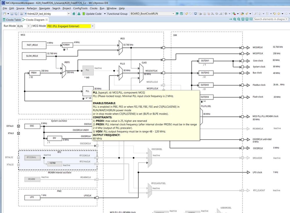
When I use the clocking tool with an 8 MHz crystal and then selecting "PEE" (PLL Engaged External), I get a default of 80 MHz. What is the correct value to change the PLL in the "MCG" block to get 120 MHz, "/2 * 30" will do it (the default is "/4 * 40") but I want to make sure this is the right/best way of doing it.
I can't seem to find this documented anywhere.
Thanx!
myke
解決済! 解決策の投稿を見る。
- 新着としてマーク
- ブックマーク
- 購読
- ミュート
- RSS フィードを購読する
- ハイライト
- 印刷
- 不適切なコンテンツを報告
Hi Mark,
Thank you for the information - I think we're talking about the same thing.
In the screen shot below, you can see you get a pop-up when you hover over the "PLL" Module (which seems to incorporate the "PRDIV" and "MCG_C6 (VDIV0) PLL" in the utasker page you referenced).
When I look in the K22 reference manual, I guess I go by "Figure 5-1. Clocking Diagram " in which there is the "PLL" box (same as the MCUXpresso diagram above) which corresponds to nothing I can cross reference in the document BUT, if I look at the utasker diagram, I can see registers MCG_5 (which houses the PRDIV0 "PLL External Reference Divider" bits) and MCG_6 (which houses the VIVO "VC0 Divider" bits which is unfortunately described as a divider when in it actually multiplies the signal coming in).
So, if I'm correctly comprehending what's provided by the reference manual, MCUXpresso and the utasker web page, the PRDIV0 bits divide the clock coming from XTAL0/EXTAL0 to 1 to 1/25th of its frequency, BUT the output must be between 2 MHz and 4 MHz (which means that for an 8 MHz crystal, like what's used on the FRDM-K22F, this can be 2 or 4), and the VDIV0 bits provide a multiplication factor of 24 to 55. The output of the "PLL" module (as NXP calls it) must be between 48 MHz and 120 MHz. Along with this, the "lock" symbol indicates that the timing is only accurate when the "LOCK0" bit is set in the MCG_S register - looking at the SDK code, the LOCK0 bit is polled in "CLOCK_EnablePll0" before it returns, where you would expect it to be.
As I will be using an 8 MHz clock in my K22 based product, like the FRDM-K22F, that means that I want to run in "PEE" mode with the PRDIV0 at 2 and the VDIV0 at 30, like was discussed before.
Anything you can see that is missing here?
Thank you for providing the link to the utasker page - that really helped cement what is happening here.
myke
- 新着としてマーク
- ブックマーク
- 購読
- ミュート
- RSS フィードを購読する
- ハイライト
- 印刷
- 不適切なコンテンツを報告
Myke
Yes, all looks to match. Note that the divider in the PLL is in the "feedback path" and this has the effect of a multiplier on the output frequency. I think you just need to somehow get the PLL to multiple by 30.
Here is the code that I use for HSRUN at 120MHz on this board and I have written the exact hex values written to the registers as reference:
MCG_C2 = (MCG_C2_FREQ_RANGE | MCG_C2_GAIN_MODE | MCG_C2_EREFS | MCG_C2_LOCRE0); // [0x94] select crystal oscillator and select a suitable range
MCG_C1 = (MCG_C1_CLKS_EXTERN_CLK | MCG_C1_FRDIV_VALUE); // [0x98] switch to external source (the FLL input clock is set to as close to its input range as possible, although this is not absolutely necessary if the FLL will not be used)
_WAIT_REGISTER_FALSE(MCG_S, MCG_S_OSCINIT); // loop until the crystal source has been selected
_WAIT_REGISTER_TRUE(MCG_S, MCG_S_IREFST); // loop until the FLL source is no longer the internal reference clock
while ((MCG_S & MCG_S_CLKST_MASK) != MCG_S_CLKST_EXTERN_CLK) {} // loop until the external reference clock source is valid
MCG_C5 = ((CLOCK_DIV - 1) | MCG_C5_PLLSTEN0); // [0x21] now move from state FEE to state PBE (or FBE) PLL remains enabled in normal stop modes
MCG_C6 = ((CLOCK_MUL - MCG_C6_VDIV0_LOWEST) | MCG_C6_PLLS); // [0x46] set the PLL multiplication factor
while ((MCG_S & MCG_S_PLLST) == 0) {} // loop until the PLLS clock source becomes valid
while ((MCG_S & MCG_S_LOCK) == 0) {} // loop until PLL locks
SIM_CLKDIV1 = (((SYSTEM_CLOCK_DIVIDE - 1) << 28) | ((BUS_CLOCK_DIVIDE - 1) << 24) | ((FLEX_CLOCK_DIVIDE - 1) << 20) | ((FLASH_CLOCK_DIVIDE - 1) << 16)); // [0x01240000] prepare bus clock divides
SMC_PMCTRL = SMC_PMCTRL_RUNM_HSRUN; // [0x60] set high speed run mode (restrictions apply) so that the clock speeds can be obtained
MCG_C1 = (MCG_C1_CLKS_PLL_FLL | MCG_C1_FRDIV_1024); // [0x28] finally move from PBE to PEE mode - switch to PLL clock
while ((MCG_S & MCG_S_CLKST_MASK) != MCG_S_CLKST_PLL) {} // loop until the PLL clock is selected
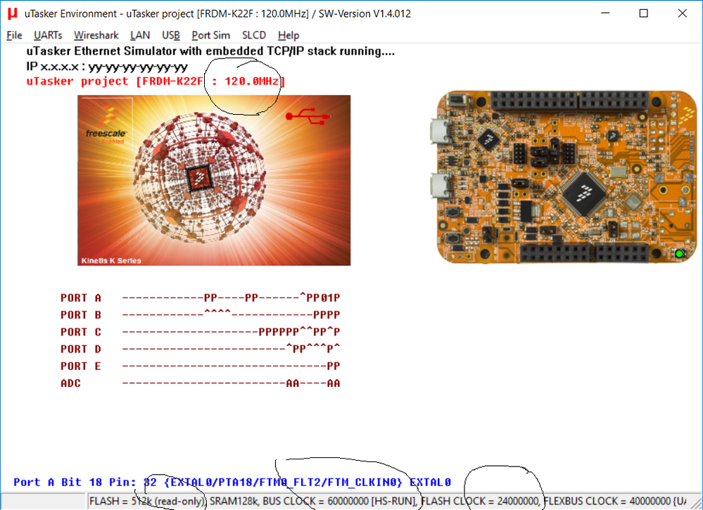
Simulation below showing the frequencies that result.
Attached is a reference binary for board (it has a memory debugger on its VCOM UART connection at 115k so you can also display register values being used).
Probably by comparing the generated code with the above you can find it more or less is equivalent and identify the value needing change, even if it can't be set in the generation tool.
Regards
Mark
[uTasker project developer for Kinetis and i.MX RT]
- 新着としてマーク
- ブックマーク
- 購読
- ミュート
- RSS フィードを購読する
- ハイライト
- 印刷
- 不適切なコンテンツを報告
Thanx!
- 新着としてマーク
- ブックマーク
- 購読
- ミュート
- RSS フィードを購読する
- ハイライト
- 印刷
- 不適切なコンテンツを報告
Hi
The K22 on the FRDM/K22F board has a maximum RUN mode speed of 80MHz and a maximum High Speed RUN mode speed of 120MHz (with some restrictions, such as Flash programming is not possible).
Probably you need to select HSRUN mode to allow the tool to configure faster than 80MHz.
Regards
Mark
[uTasker project developer for Kinetis and i.MX RT]
- 新着としてマーク
- ブックマーク
- 購読
- ミュート
- RSS フィードを購読する
- ハイライト
- 印刷
- 不適切なコンテンツを報告
Hi Mark,
Thank you for the suggestion but changing to "HSRUN" doesn't change the Core Clock rate.
myke
- 新着としてマーク
- ブックマーク
- 購読
- ミュート
- RSS フィードを購読する
- ハイライト
- 印刷
- 不適切なコンテンツを報告
Myke
I don't use the configuration tools, but these are the HSRUN mode settings I use on the FRDM-K22F for 120MHz CPU speed:
#define CRYSTAL_FREQUENCY 8000000 // 8 MHz crystal on board
#define USE_HIGH_SPEED_RUN_MODE // operate in high speed RUN mode - note that flash programing is not possible in this mode so NO_FLASH_SUPPORT should be enabled in config.h
#define CLOCK_DIV 2 // input must be divided to 2MHz..4MHz range (/1 to /24)
#define CLOCK_MUL 30 // the PLL multiplication factor to achieve operating frequency of 120MHz (x24 to x55 possible) - > 80MHz requires high speed run mode, which doesn't allow flash programming
#define FLEX_CLOCK_DIVIDE 3 // 120/3 to give 40MHz
#define FLASH_CLOCK_DIVIDE 5 // 120/5 to give 24MHz
#define BUS_CLOCK_DIVIDE 2 // 120/2 to give 60MHz
So if you are presently getting 80MHz you need to find a way to change the clock multiplication value (within its possible range). Probably it is giving you an input divide of 4 and multiplication of 40 so you need to change the divider to 2 and mul to 30 as above. See the following if you are not familiar with the MCG:
https://www.utasker.com/kinetis/MCG.html
Regards
Mark
[uTasker project developer for Kinetis and i.MX RT]

