
- Forums
- Product Forums
- General Purpose MicrocontrollersGeneral Purpose Microcontrollers
- i.MX Forumsi.MX Forums
- QorIQ Processing PlatformsQorIQ Processing Platforms
- Identification and SecurityIdentification and Security
- Power ManagementPower Management
- Wireless ConnectivityWireless Connectivity
- RFID / NFCRFID / NFC
- Advanced AnalogAdvanced Analog
- Neural Processing UnitsNeural Processing Units
- MCX Microcontrollers
- S32G
- S32K
- S32V
- MPC5xxx
- Other NXP Products
- S12 / MagniV Microcontrollers
- Powertrain and Electrification Analog Drivers
- Sensors
- Vybrid Processors
- Digital Signal Controllers
- 8-bit Microcontrollers
- ColdFire/68K Microcontrollers and Processors
- PowerQUICC Processors
- OSBDM and TBDML
- S32M
- S32Z/E
-
- Solution Forums
- Software Forums
- MCUXpresso Software and ToolsMCUXpresso Software and Tools
- CodeWarriorCodeWarrior
- MQX Software SolutionsMQX Software Solutions
- Model-Based Design Toolbox (MBDT)Model-Based Design Toolbox (MBDT)
- FreeMASTER
- eIQ Machine Learning Software
- Embedded Software and Tools Clinic
- S32 SDK
- S32 Design Studio
- GUI Guider
- Zephyr Project
- Voice Technology
- Application Software Packs
- Secure Provisioning SDK (SPSDK)
- Processor Expert Software
- Generative AI & LLMs
-
- Topics
- Mobile Robotics - Drones and RoversMobile Robotics - Drones and Rovers
- NXP Training ContentNXP Training Content
- University ProgramsUniversity Programs
- Rapid IoT
- NXP Designs
- SafeAssure-Community
- OSS Security & Maintenance
- Using Our Community
-
- Cloud Lab Forums
-
- Knowledge Bases
- ARM Microcontrollers
- i.MX Processors
- Identification and Security
- Model-Based Design Toolbox (MBDT)
- QorIQ Processing Platforms
- S32 Automotive Processing Platform
- Wireless Connectivity
- CodeWarrior
- MCUXpresso Suite of Software and Tools
- MQX Software Solutions
- RFID / NFC
- Advanced Analog
- Neural Processing Units
-
- NXP Tech Blogs
- Home
- :
- i.MX Forums
- :
- i.MX Processors
- :
- LPDDR2 pin swapping on i.MX6DL, can or not?
LPDDR2 pin swapping on i.MX6DL, can or not?
- Subscribe to RSS Feed
- Mark Topic as New
- Mark Topic as Read
- Float this Topic for Current User
- Bookmark
- Subscribe
- Mute
- Printer Friendly Page
LPDDR2 pin swapping on i.MX6DL, can or not?

- Mark as New
- Bookmark
- Subscribe
- Mute
- Subscribe to RSS Feed
- Permalink
- Report Inappropriate Content
Hi
I would like to use e.MCP(Kingston 08EMCP08-NL2CV100-C50) which is e.MMC 8GB + LPDDR2 8Gbit on our i.MX platform .
In order to do easy pcb routing, can I swap data bus?
I have checked this topic :LPDDR2 pin swapping on iMx6DL he's answer is NO, but I found another reference design which is MX6QCPULPDDR2, They do swap data bus .I don't know who is correct..
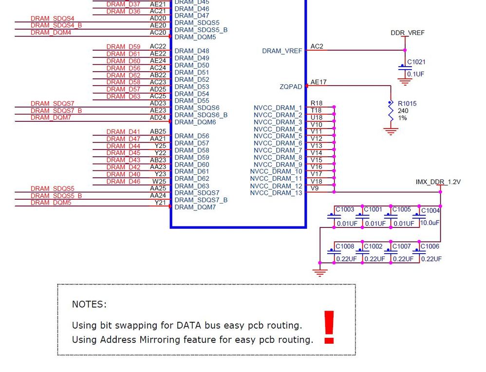
Could anyone help me?
Thanks,

 igorpadykov
- Mark as New
- Bookmark
- Subscribe
- Mute
- Subscribe to RSS Feed
- Permalink
- Report Inappropriate Content
Hi Elliot
answer on topic was based on http://www.jedec.org/sites/default/files/docs/JESD209-2B.pdf
and implies usage LPDDR2 memory subsystem that includes both NVM and SDRAM memories,
as mentioned in Annex B "LPDDR2-NVM Boot Procedure" :
Because LPDDR2 devices (both DRAM and NVM) assign specific
functions to the different byte lanes of the data bus and even to specific bits within the
bytes, byte and bit swapping shall be avoided.
If this is only LPDRR2 chip, as in MX6QCPULPDDR2 reference design, seems
no problem with swapping.
Best regards
igor
-----------------------------------------------------------------------------------------------------------------------
Note: If this post answers your question, please click the Correct Answer button. Thank you!
-----------------------------------------------------------------------------------------------------------------------
- Mark as New
- Bookmark
- Subscribe
- Mute
- Subscribe to RSS Feed
- Permalink
- Report Inappropriate Content
Hi igor
According to your document, I saw a note from page 9:
"NOTE 2 Ordering of DQ bits shall be maintained in the system, including within the package and on the PCB. DQ byte swapping and DQ bit Swapping are not allowed in the system."
That means DQ can't be swapped, right?
So I can't do this? JUST swap DQ BYTE.
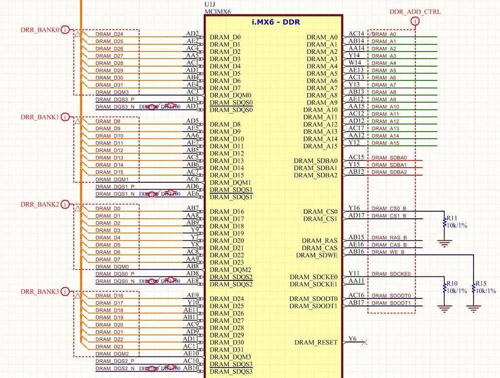
Elliott
igorpadykov
- Mark as New
- Bookmark
- Subscribe
- Mute
- Subscribe to RSS Feed
- Permalink
- Report Inappropriate Content
Hi Elliot
you are right, strictly following jedec this is prohibited.
Also it may be useful to look at
Zynq LPDDR2 DQ Swap Question - Community Forums
Best regards
igor
- Mark as New
- Bookmark
- Subscribe
- Mute
- Subscribe to RSS Feed
- Permalink
- Report Inappropriate Content
Hi igor
Thanks for you reply,
but the i.MX6DL can't set the DQ bus by software(uboot/kernel)?
PCB layout is so hard for implement without DQ bus changing .
Elliott
igorpadykov
- Mark as New
- Bookmark
- Subscribe
- Mute
- Subscribe to RSS Feed
- Permalink
- Report Inappropriate Content
Hi Elliot
I think if Mode Reg Read is not used, then swapping
can be used, as described on link.
~igor
