- Forums
- Product Forums
- General Purpose MicrocontrollersGeneral Purpose Microcontrollers
- i.MX Forumsi.MX Forums
- QorIQ Processing PlatformsQorIQ Processing Platforms
- Identification and SecurityIdentification and Security
- Power ManagementPower Management
- Wireless ConnectivityWireless Connectivity
- RFID / NFCRFID / NFC
- Advanced AnalogAdvanced Analog
- MCX Microcontrollers
- S32G
- S32K
- S32V
- MPC5xxx
- Other NXP Products
- S12 / MagniV Microcontrollers
- Powertrain and Electrification Analog Drivers
- Sensors
- Vybrid Processors
- Digital Signal Controllers
- 8-bit Microcontrollers
- ColdFire/68K Microcontrollers and Processors
- PowerQUICC Processors
- OSBDM and TBDML
- S32M
- S32Z/E
-
- Solution Forums
- Software Forums
- MCUXpresso Software and ToolsMCUXpresso Software and Tools
- CodeWarriorCodeWarrior
- MQX Software SolutionsMQX Software Solutions
- Model-Based Design Toolbox (MBDT)Model-Based Design Toolbox (MBDT)
- FreeMASTER
- eIQ Machine Learning Software
- Embedded Software and Tools Clinic
- S32 SDK
- S32 Design Studio
- GUI Guider
- Zephyr Project
- Voice Technology
- Application Software Packs
- Secure Provisioning SDK (SPSDK)
- Processor Expert Software
- Generative AI & LLMs
-
- Topics
- Mobile Robotics - Drones and RoversMobile Robotics - Drones and Rovers
- NXP Training ContentNXP Training Content
- University ProgramsUniversity Programs
- Rapid IoT
- NXP Designs
- SafeAssure-Community
- OSS Security & Maintenance
- Using Our Community
-
- Cloud Lab Forums
-
- Knowledge Bases
- ARM Microcontrollers
- i.MX Processors
- Identification and Security
- Model-Based Design Toolbox (MBDT)
- QorIQ Processing Platforms
- S32 Automotive Processing Platform
- Wireless Connectivity
- CodeWarrior
- MCUXpresso Suite of Software and Tools
- MQX Software Solutions
- RFID / NFC
- Advanced Analog
-
- NXP Tech Blogs
- Home
- :
- General Purpose Microcontrollers
- :
- Kinetis Microcontrollers
- :
- Reset error, debugging KW41Z with an external J-link Base tool
Reset error, debugging KW41Z with an external J-link Base tool
- Subscribe to RSS Feed
- Mark Topic as New
- Mark Topic as Read
- Float this Topic for Current User
- Bookmark
- Subscribe
- Mute
- Printer Friendly Page
- Mark as New
- Bookmark
- Subscribe
- Mute
- Subscribe to RSS Feed
- Permalink
- Report Inappropriate Content
Hi,
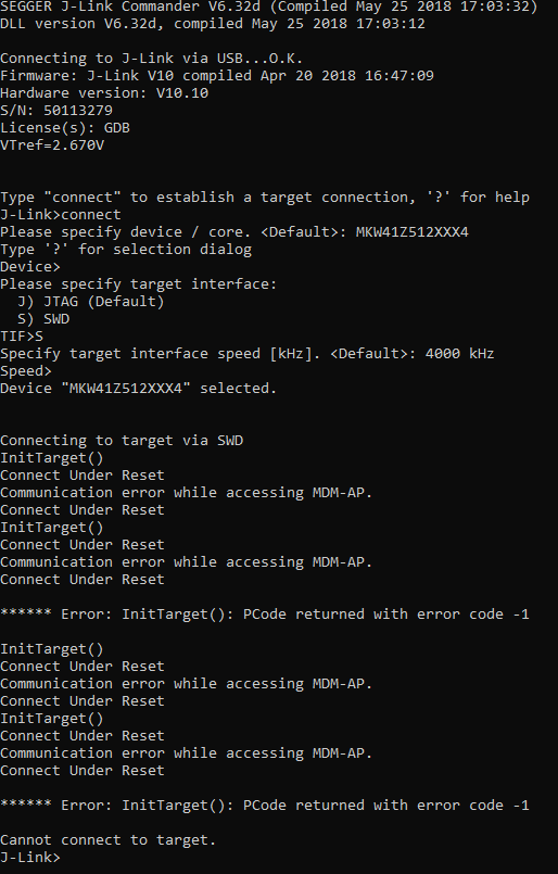
I have a Rigado Module R41Z (based on KW41Z) solded in a custom board. I want to debug it with an external J-Link debugger via SWD, but all the time im getting this response from J-Link software as well from Kinetis Design Studio IDE, when I try to debug it with a custom program:
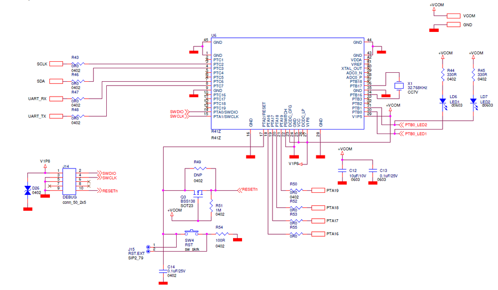
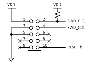
The schematic from SWD and the R41Z module is the following:
The module is powered by 2.6V, can be the low power the cause of this error?
It is the reset button connection the error?
With this J-Link tool I am able to program KW41Z Eval module without problem, I do not program them with Open-SDA firmware, so I hope the J-Link debugger are not the cause of the problem.
I would appreciate a solution of this problem, I can not program my board if I do not fix it.
Best,
Diego C.
Solved! Go to Solution.
- Mark as New
- Bookmark
- Subscribe
- Mute
- Subscribe to RSS Feed
- Permalink
- Report Inappropriate Content
Hi Diego,
The mass erase is triggered by the "unlock kinetis" command. However, in your case the error “ERROR: Read from DP/AP register failed!” tells us that the debugger is not even able to correctly communicate with the debug port of the KW41Z. My suggestion is to check all your hardware connections and make sure with an oscilloscope that the expected signals are clean and noise free at the R41Z module SWD pins.
Do you have more R41Z modules available? If you have multiple boards, you could compare the behavior between them and if each board behaves differently, there could be a HW issue during your assembly process.
Additionally, you can refer to the following thread Communication error while accessing MDM-AP. and follow the "Kinetis Lock issue analysis and unlock way" document.
Let me know your results.
Regards,
Gerardo
- Mark as New
- Bookmark
- Subscribe
- Mute
- Subscribe to RSS Feed
- Permalink
- Report Inappropriate Content
Hi Gerardo,
I changed the test to my second custom board, I didn't perform any SW or HW change and "unlock kinetis" worked well and I was able to connect to my board. So I think the error was due to Hardware as Gerardo said. Everyone that have "Read from DP/AP Register failed" IT IS DUE TO HW!
I really appreciate your help Gerardo,
Regards,
Diego C.
- Mark as New
- Bookmark
- Subscribe
- Mute
- Subscribe to RSS Feed
- Permalink
- Report Inappropriate Content
Happy to help! :smileyhappy:
Thanks for letting us know your results.
- Mark as New
- Bookmark
- Subscribe
- Mute
- Subscribe to RSS Feed
- Permalink
- Report Inappropriate Content
Hi Diego,
The mass erase is triggered by the "unlock kinetis" command. However, in your case the error “ERROR: Read from DP/AP register failed!” tells us that the debugger is not even able to correctly communicate with the debug port of the KW41Z. My suggestion is to check all your hardware connections and make sure with an oscilloscope that the expected signals are clean and noise free at the R41Z module SWD pins.
Do you have more R41Z modules available? If you have multiple boards, you could compare the behavior between them and if each board behaves differently, there could be a HW issue during your assembly process.
Additionally, you can refer to the following thread Communication error while accessing MDM-AP. and follow the "Kinetis Lock issue analysis and unlock way" document.
Let me know your results.
Regards,
Gerardo
- Mark as New
- Bookmark
- Subscribe
- Mute
- Subscribe to RSS Feed
- Permalink
- Report Inappropriate Content
Hi Gerardo, Hi Edgar,
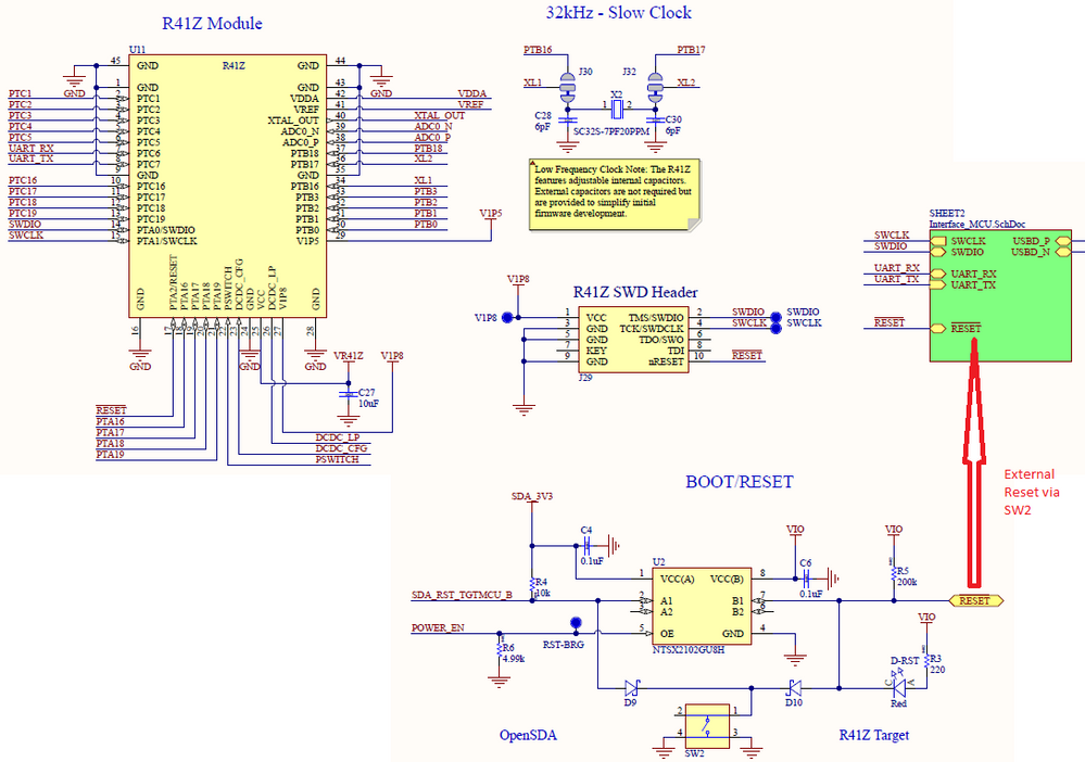
I really appreciate your help. The transistor circuit was to make a little protection between the reset pin of the SWD header and the reset pin of the KW41Z module (I have now deleted it and have connected directly Reset SWD pin to Reset KW41Z pin). To perform the SWD connections I have followed the schematics of the R41Z-Eval-Board (I have 4 Eval Board which I tried to debug via SWD with my J-link tool and it works properly). The SWD connections from this board are:
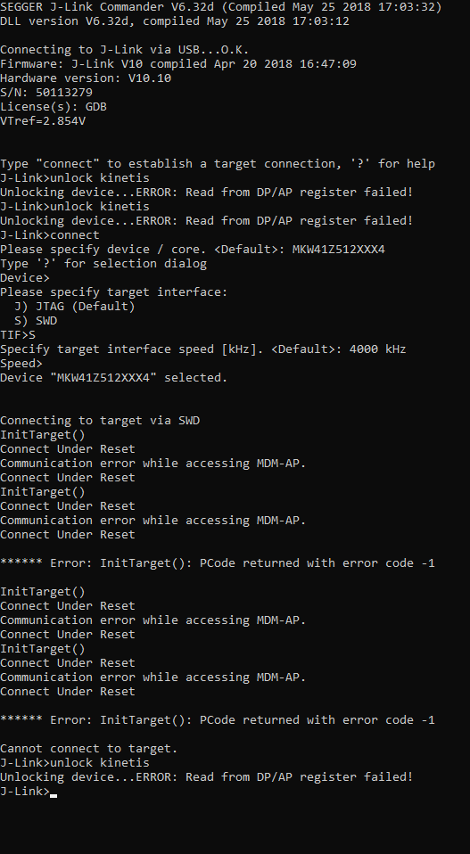
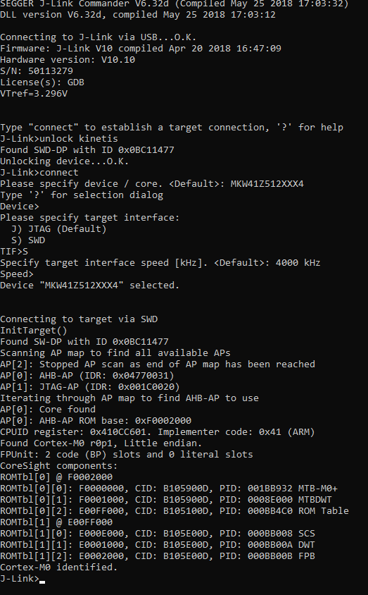
I also taped "unlock kinetis" before taping the command "connect" to the J-link commander and the problem still exists. New error appears when I write "unlock kinetis", ERROR: Read from DP/AP register failed:
When I take a R41Z-Eval-Board and I debug it via SWD with the J-link tool and tape the same commands as before everything works ok, so the problem is the KW41Z blank module of my custom board:
I think my problem is related with the default configuration of a blank KW41Z modules. I have found in MKW41Z Reference Manual that the blank modules are by default in secure flash state, so they can not be debugged via SWD until we do not perform a "mass erase" to the flash memory.
The reset signal behaviour is a normal behaviour from blank chips, I searched on the forum and people say that when we flash the module for first time the reset signal strange behaviour dissapear.
My problem is: How do I perform a "mass erase" to the flash memory to solve my issue? Is the "mass erase" the solution or it is related to the hardware or many other things? I am using MCUExpresso IDE or Kinetis Design Studio IDE to debug the modules, this IDE is able to perform "mass erase"?
I need to solve this problem to perform a big Thread mesh in my compnay with our custom board with KW41Z modules.
I really hope you can solve it.
Best,
Diego C.
- Mark as New
- Bookmark
- Subscribe
- Mute
- Subscribe to RSS Feed
- Permalink
- Report Inappropriate Content
Hello Diego,
What is the purpose of the transistor circuit connected to the reset pin of the target MCU?
The pin 10 from the debug header should be connected directly to the reset pin and pin 9 should be left floating but you have it tied to ground. Try these changes and let me know your results.
Additionally, have you tried the "unlock kinetis" command in the J-Link commander? Does it throw the same error?
Regards
- Mark as New
- Bookmark
- Subscribe
- Mute
- Subscribe to RSS Feed
- Permalink
- Report Inappropriate Content
Hi Diego
The debug signals (SWD_CLK and SWD_DIO) are multiplexed with general purpose I/O pins, therefore will require proper biasing to select the operating mode. It's highly recommended connect an external pull up resistor in SWD_DIO pin as shown below:
For more information I'll give you this documentation, please visit 2.1.5.1 Debug interface:
Best regards.
- Mark as New
- Bookmark
- Subscribe
- Mute
- Subscribe to RSS Feed
- Permalink
- Report Inappropriate Content
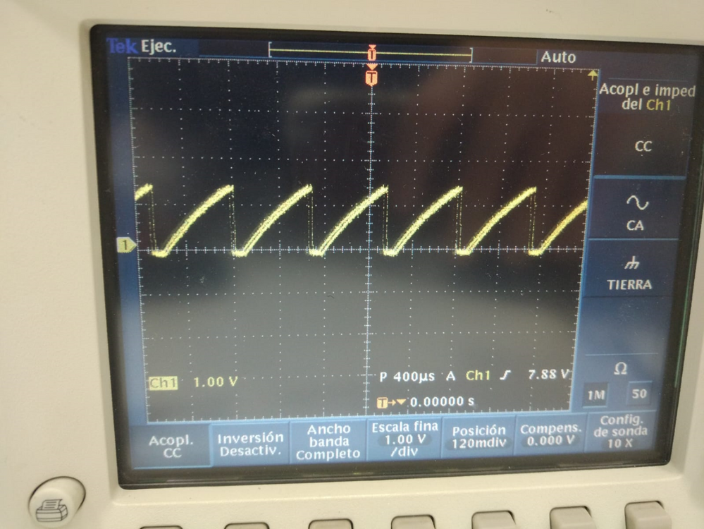
I attacthed below the Reset signal from the KW41Z:
So I think the KW41Z is continuously resseting maybe it is the cause of the error. When I plug the J-Link tool in order to debug the module I obtain the message "Connect under reset", "Communication error while accessing MDM-AP" and the J-Link LED turn red (because it is always resseting).
How can I solve this problem? Please I really need a solution.
Diego C.
