- Forums
- Product Forums
- General Purpose MicrocontrollersGeneral Purpose Microcontrollers
- i.MX Forumsi.MX Forums
- QorIQ Processing PlatformsQorIQ Processing Platforms
- Identification and SecurityIdentification and Security
- Power ManagementPower Management
- Wireless ConnectivityWireless Connectivity
- RFID / NFCRFID / NFC
- Advanced AnalogAdvanced Analog
- MCX Microcontrollers
- S32G
- S32K
- S32V
- MPC5xxx
- Other NXP Products
- S12 / MagniV Microcontrollers
- Powertrain and Electrification Analog Drivers
- Sensors
- Vybrid Processors
- Digital Signal Controllers
- 8-bit Microcontrollers
- ColdFire/68K Microcontrollers and Processors
- PowerQUICC Processors
- OSBDM and TBDML
- S32M
- S32Z/E
-
- Solution Forums
- Software Forums
- MCUXpresso Software and ToolsMCUXpresso Software and Tools
- CodeWarriorCodeWarrior
- MQX Software SolutionsMQX Software Solutions
- Model-Based Design Toolbox (MBDT)Model-Based Design Toolbox (MBDT)
- FreeMASTER
- eIQ Machine Learning Software
- Embedded Software and Tools Clinic
- S32 SDK
- S32 Design Studio
- GUI Guider
- Zephyr Project
- Voice Technology
- Application Software Packs
- Secure Provisioning SDK (SPSDK)
- Processor Expert Software
- Generative AI & LLMs
-
- Topics
- Mobile Robotics - Drones and RoversMobile Robotics - Drones and Rovers
- NXP Training ContentNXP Training Content
- University ProgramsUniversity Programs
- Rapid IoT
- NXP Designs
- SafeAssure-Community
- OSS Security & Maintenance
- Using Our Community
-
- Cloud Lab Forums
-
- Knowledge Bases
- ARM Microcontrollers
- i.MX Processors
- Identification and Security
- Model-Based Design Toolbox (MBDT)
- QorIQ Processing Platforms
- S32 Automotive Processing Platform
- Wireless Connectivity
- CodeWarrior
- MCUXpresso Suite of Software and Tools
- MQX Software Solutions
- RFID / NFC
- Advanced Analog
-
- NXP Tech Blogs
- Home
- :
- i.MX Forums
- :
- i.MX RT Crossover MCUs
- :
- Re: Cannot understand how XIP FlexSPI configuration could work on IMXRT1060-EVKB
Cannot understand how XIP FlexSPI configuration could work on IMXRT1060-EVKB
- Subscribe to RSS Feed
- Mark Topic as New
- Mark Topic as Read
- Float this Topic for Current User
- Bookmark
- Subscribe
- Mute
- Printer Friendly Page
- Mark as New
- Bookmark
- Subscribe
- Mute
- Subscribe to RSS Feed
- Permalink
- Report Inappropriate Content
Hello,
I can't truly understand how the configuration coming with XIP examples on IMXRT1060-EVKB could work with IS25WP064 QSPI Flash memory.
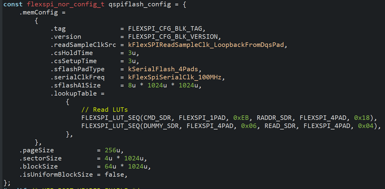
Provided configuration is the following:
from where it's clear that LUT command setup here at index 0, corresponding to the read command according to Table 22-2 in Reference Manual, is 0xEB which corresponds to Fast Read Quad I/O Operation from IS25WP064 datasheet while there's no evidence about if, where and how QE (Quad-Enable) bit is set in status register to enable the use of such quad-read operation.
Solved! Go to Solution.
- Mark as New
- Bookmark
- Subscribe
- Mute
- Subscribe to RSS Feed
- Permalink
- Report Inappropriate Content
After months of discussion with Omar from NXP Tech Support, I would like to share his (incomplete, sadly) explanation with you. I really don't know why NXP wouldn't participate so much in public threads like this, to share knowledge to as much people as possible at the same time... but, this is it.
"It is possible that this QE bit is set on the flash driver (CFX file) on McuXpresso. Unfortunately, it is not possible to get the source file to confirm this, those source files are not available for the public."
- Mark as New
- Bookmark
- Subscribe
- Mute
- Subscribe to RSS Feed
- Permalink
- Report Inappropriate Content
Hi @SpoonMan
Here is a correction for my previous comment. Sorry for the inconvenience.
Enabling quad mode operations is something that needs to be done before hand. For example there is a bit that needs to be programmed a single time on the memory. Boot rom will attempt to communicate with the memory by using LUT commands, and those commands now can be for quad mode.
Diego
- Mark as New
- Bookmark
- Subscribe
- Mute
- Subscribe to RSS Feed
- Permalink
- Report Inappropriate Content
Hi @diego_charles!
Hope you're doing well
I sadly have to say you're still not answering to my question... Please, check the screenshot in heading post, you can see by your eyes that XIP read command in LUT is configured as:
FLEXSPI_LUT_SEQ(CMD_SDR, FLEXSPI_1PAD, 0xEB, RADDR_SDR, FLEXSPI_4PAD, 0x18),
FLEXSPI_LUT_SEQ(DUMMY_SDR, FLEXSPI_4PAD, 0x06, READ_SDR, FLEXSPI_4PAD, 0x04),
which means that FAST READ QUAD I/O command is configured to send address, dummy cycles and read data on 4 lines, and according to IS25WP512M Flash memory datasheet:
QE bit in Status Register must be set before sending such instruction.
So, the question is... how is this possible? Who, when and where is sending Write Status Register command with appropriate QE bit set?
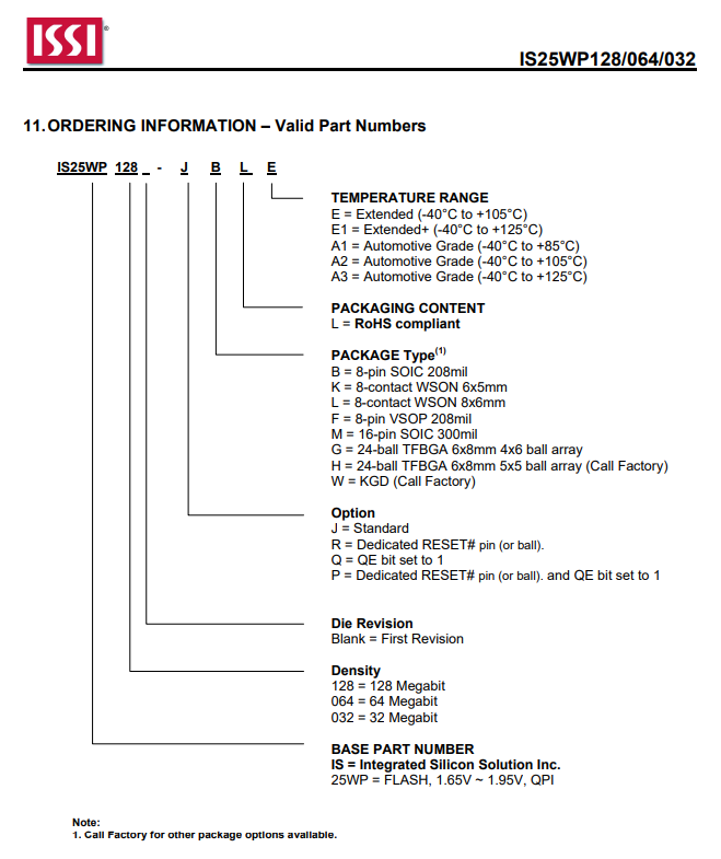
P.S. Yes, I know IS25WP512M is not the standard Flash mounted on eval board, but IS25WP064AJBLE should be the same because J means "standard" and not "QE=1 by factory" according the datasheet:
- Mark as New
- Bookmark
- Subscribe
- Mute
- Subscribe to RSS Feed
- Permalink
- Report Inappropriate Content
Hi @SpoonMan
I hope you are doing well!
I am sorry for the lack of details, but per my knowledge the bootROM does the job to send Quad mode command to the flash memory during MCU boot.
Best regards,
Diego
- Mark as New
- Bookmark
- Subscribe
- Mute
- Subscribe to RSS Feed
- Permalink
- Report Inappropriate Content
Hi @diego_charles ,
hope you're doing well too! Sorry if the following question may look weird, but... from where did you get this information?
According to another thread:
@jeremyzhou was asserting that QE can be set during application time like in flexspi_nor_polling_transfer demo and that we all are encouraged to follow that example code, but this is not what I'm asking. My question is basically the same as the one asked by @ju-hakpark in the thread I linked, which is: how and where is QE configured before XIP takes place? (and how can I see/edit such configuration, for example to enable 4-byte addressing too?)
Thanks in advance for your help
Best regards!
- Mark as New
- Bookmark
- Subscribe
- Mute
- Subscribe to RSS Feed
- Permalink
- Report Inappropriate Content
- Mark as New
- Bookmark
- Subscribe
- Mute
- Subscribe to RSS Feed
- Permalink
- Report Inappropriate Content
- Mark as New
- Bookmark
- Subscribe
- Mute
- Subscribe to RSS Feed
- Permalink
- Report Inappropriate Content
Hello @kef2
I know that QE could be stored in flash memory at non-volatile registers. The point is that I noticed that demos are working using quad read in XIP LUT even if I don't set QE explicitly in volatile and/or non-volatile registers, and even if I de-solder existing chip on EVK and solder a new one.
This is the meaning of the topic. Hope that now it's more clear to you too.
- Mark as New
- Bookmark
- Subscribe
- Mute
- Subscribe to RSS Feed
- Permalink
- Report Inappropriate Content
Demos are just demos, remove QE if you are not using quad mode. Simple.
- Mark as New
- Bookmark
- Subscribe
- Mute
- Subscribe to RSS Feed
- Permalink
- Report Inappropriate Content
The point is NOT I don't need QE, the point is I would like to UNDERSTAND who, when and where is setting QE. Understanding is everything if your goal is to develop rock-solid platforms and applications.
I hope that now it's clear the point of this topic.
- Mark as New
- Bookmark
- Subscribe
- Mute
- Subscribe to RSS Feed
- Permalink
- Report Inappropriate Content
Do you imply that you had really blank flash chip, with non volatile QE bit unprogrammed, and demo, which isn't programming QE works well in quad mode? So, wasn't QE programmed before you launched your app for the first time?
- Mark as New
- Bookmark
- Subscribe
- Mute
- Subscribe to RSS Feed
- Permalink
- Report Inappropriate Content


