- Forums
- Product Forums
- General Purpose MicrocontrollersGeneral Purpose Microcontrollers
- i.MX Forumsi.MX Forums
- QorIQ Processing PlatformsQorIQ Processing Platforms
- Identification and SecurityIdentification and Security
- Power ManagementPower Management
- Wireless ConnectivityWireless Connectivity
- RFID / NFCRFID / NFC
- MCX Microcontrollers
- S32G
- S32K
- S32V
- MPC5xxx
- Other NXP Products
- S12 / MagniV Microcontrollers
- Powertrain and Electrification Analog Drivers
- Sensors
- Vybrid Processors
- Digital Signal Controllers
- 8-bit Microcontrollers
- ColdFire/68K Microcontrollers and Processors
- PowerQUICC Processors
- OSBDM and TBDML
- S32M
-
- Solution Forums
- Software Forums
- MCUXpresso Software and ToolsMCUXpresso Software and Tools
- CodeWarriorCodeWarrior
- MQX Software SolutionsMQX Software Solutions
- Model-Based Design Toolbox (MBDT)Model-Based Design Toolbox (MBDT)
- FreeMASTER
- eIQ Machine Learning Software
- Embedded Software and Tools Clinic
- S32 SDK
- S32 Design Studio
- GUI Guider
- Zephyr Project
- Voice Technology
- Application Software Packs
- Secure Provisioning SDK (SPSDK)
- Processor Expert Software
-
- Topics
- Mobile Robotics - Drones and RoversMobile Robotics - Drones and Rovers
- NXP Training ContentNXP Training Content
- University ProgramsUniversity Programs
- Rapid IoT
- NXP Designs
- SafeAssure-Community
- OSS Security & Maintenance
- Using Our Community
-
- Cloud Lab Forums
-
- Knowledge Bases
- ARM Microcontrollers
- i.MX Processors
- Identification and Security
- Model-Based Design Toolbox (MBDT)
- QorIQ Processing Platforms
- S32 Automotive Processing Platform
- Wireless Connectivity
- CodeWarrior
- MCUXpresso Suite of Software and Tools
- MQX Software Solutions
- RFID / NFC
-
- Home
- :
- i.MXプロセッサ
- :
- i.MX RT Crossover MCUs Knowledge Base
- :
- i.MXRT1050 SDRAM Clock Configuration
i.MXRT1050 SDRAM Clock Configuration
- RSS フィードを購読する
- 新着としてマーク
- 既読としてマーク
- ブックマーク
- 購読
- 印刷用ページ
- 不適切なコンテンツを報告
i.MXRT1050 SDRAM Clock Configuration
i.MXRT1050 SDRAM Clock Configuration
- The path of SDRAM Clock in Clock Tree
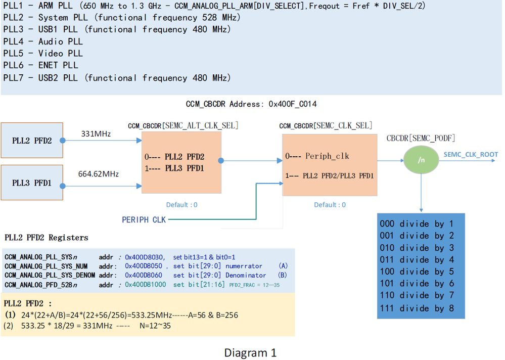
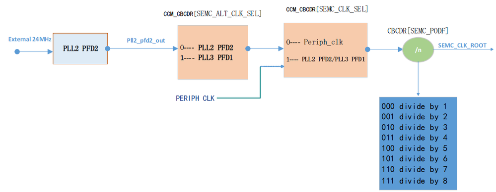
According CCM clock tree in i.MXRT1050 reference manual, we can abstract part of SDRAM clock, and draw it’s diagram below.

- Descriptions for Diagram 1
(1) PLL2 PFD2

① Registers related to PLL2 PFD2
---CCM_ANALOG_PLL_SYSn (page 767, in reference manual)
Address: 0x400D_8030h
important bits:
bit[15:14]---- select clock source.
Bit[13] ----- Enable PLL output
Bit[0]------- This field controls the PLL loop divider. 0 - Fout=Fref*20; 1 - Fout=Fref*22.
---CCM_ANALOG_PLL_SYS_NUM(page 768, in reference manual)
Address: 0x400D_8050h
important bits:
bit[29:0]--- 30 bit numerator (A) of fractional loop divider (signed integer)
---CCM_ANALOG_PLL_SYS_DENOM (page 769, in reference manual)
Address: 0x400D_8060h
important bits:
bit[29:0]---- 30 bit Denominator (B) of fractional loop divider (unsigned integer).
---CCM_ANALOG_PFD_528n (page 769, in reference manual)
Address: 0x400D_8100h
important bits:
bit[21:16]----- This field controls the fractional divide value. The resulting frequency shall be 528*18/PFD2_FRAC where PFD2_FRAC is in the range 12-35.
② Computational formula
PLL2_PFD2_OUT=(External 24MHz)*(Fout + A/B) * 18/ PFD2_FRAC
③ Example for PLL2_PFD2_OUT computation
CCM_ANALOG_PLL_SYSn[0] = 1 // Fout=Fref*22
CCM_ANALOG_PLL_SYS_NUM[29:0] = 56 // A = 56
CCM_ANALOG_PLL_SYS_DENOM[29:0] = 256 // B=256
CCM_ANALOG_PFD_528n[21:16] = 29 // PFD2_FRAC=29
PLL2_PFD2_OUT = 24 * (22 + 56/256)*18/29 = 331MHz (330.98MHz)
(2) Clock Select Register : CCM_CBCDR
Address: 0x 400F_C014h
important bits: SEMC_ALT_CLK_SEL & SEMC_CLK_SEL & SEMC_PODF
bit[7] --- bit[SEMC_ALT_CLK_SEL]
0---PLL2 PFD2 will be selected as alternative clock for SEMC root clock
1---PLL3 PFD1 will be selected as alternative clock for SEMC root clock
Bit[6] --- bit[SEMC_CLK_SEL]
0----Periph_clk output will be used as SEMC clock root
1----SEMC alternative clock will be used as SEMC clock root
Bit[18:16] --- bit[SEMC_PODF]
Post divider for SEMC clock.
NOTE: Any change of this divider might involve handshake with EMI. See CDHIPR register for the
handshake busy bits.
000 divide by 1
001 divide by 2
010 divide by 3
011 divide by 4
100 divide by 5
101 divide by 6
110 divide by 7
111 divide by 8
- Example for configuration of SDRAM Clock
Example : 166MHz SDRAM Clock
---- 0x400D8030 = 0x00002001 // wirte 0x00002001 to CCM_ANALOG_PLL_SYSn
---- 0x400D8050 = 0x00000038 // write 0x00000038 to CCM_ANALOG_PLL_SYS_NUM
---- 0x400D8060 = 0x00000100 // write 0x00000100 to CCM_ANALOG_PLL_SYS_DENOM
---- 0x400D8100 = 0x001d0000 // write 0x001d0000 to CCM_ANALOG_PFD_528n
---- 0x400FC014 = 0x00010D40 // write 0x00010D40 to CCM_CBCDR, divided by 2
NXP TIC team
Weidong Sun
2018-06-01


