- Forums
- Product Forums
- General Purpose MicrocontrollersGeneral Purpose Microcontrollers
- i.MX Forumsi.MX Forums
- QorIQ Processing PlatformsQorIQ Processing Platforms
- Identification and SecurityIdentification and Security
- Power ManagementPower Management
- Wireless ConnectivityWireless Connectivity
- RFID / NFCRFID / NFC
- Advanced AnalogAdvanced Analog
- MCX Microcontrollers
- S32G
- S32K
- S32V
- MPC5xxx
- Other NXP Products
- S12 / MagniV Microcontrollers
- Powertrain and Electrification Analog Drivers
- Sensors
- Vybrid Processors
- Digital Signal Controllers
- 8-bit Microcontrollers
- ColdFire/68K Microcontrollers and Processors
- PowerQUICC Processors
- OSBDM and TBDML
- S32M
- S32Z/E
-
- Solution Forums
- Software Forums
- MCUXpresso Software and ToolsMCUXpresso Software and Tools
- CodeWarriorCodeWarrior
- MQX Software SolutionsMQX Software Solutions
- Model-Based Design Toolbox (MBDT)Model-Based Design Toolbox (MBDT)
- FreeMASTER
- eIQ Machine Learning Software
- Embedded Software and Tools Clinic
- S32 SDK
- S32 Design Studio
- GUI Guider
- Zephyr Project
- Voice Technology
- Application Software Packs
- Secure Provisioning SDK (SPSDK)
- Processor Expert Software
- Generative AI & LLMs
-
- Topics
- Mobile Robotics - Drones and RoversMobile Robotics - Drones and Rovers
- NXP Training ContentNXP Training Content
- University ProgramsUniversity Programs
- Rapid IoT
- NXP Designs
- SafeAssure-Community
- OSS Security & Maintenance
- Using Our Community
-
- Cloud Lab Forums
-
- Knowledge Bases
- ARM Microcontrollers
- i.MX Processors
- Identification and Security
- Model-Based Design Toolbox (MBDT)
- QorIQ Processing Platforms
- S32 Automotive Processing Platform
- Wireless Connectivity
- CodeWarrior
- MCUXpresso Suite of Software and Tools
- MQX Software Solutions
- RFID / NFC
- Advanced Analog
-
- NXP Tech Blogs
- Home
- :
- i.MX Forums
- :
- i.MX Processors
- :
- Re: QSPI header config file
QSPI header config file
- Subscribe to RSS Feed
- Mark Topic as New
- Mark Topic as Read
- Float this Topic for Current User
- Bookmark
- Subscribe
- Mute
- Printer Friendly Page
- Mark as New
- Bookmark
- Subscribe
- Mute
- Subscribe to RSS Feed
- Permalink
- Report Inappropriate Content
mfgTools provide three files:
qspi-nor-macronix-mx25l51245g-config
qspi-nor-micron-n25q256a-config
qspi-nor-spansion-s25fl128s-config
thoes files are not match my flash (mx6ull + S25FL256S_64K).
how to modify thoes files to fit S25FL256S
thanks
Solved! Go to Solution.
- Mark as New
- Bookmark
- Subscribe
- Mute
- Subscribe to RSS Feed
- Permalink
- Report Inappropriate Content
Hi jianlei
please refer to Table 8-23. QuadSPI Configuration Parameters
i.MX6UL Reference Manual
http://www.nxp.com/docs/en/reference-manual/IMX6ULRM.pdf
Best regards
igor
-----------------------------------------------------------------------------------------------------------------------
Note: If this post answers your question, please click the Correct Answer button. Thank you!
-----------------------------------------------------------------------------------------------------------------------
- Mark as New
- Bookmark
- Subscribe
- Mute
- Subscribe to RSS Feed
- Permalink
- Report Inappropriate Content
Hi igor
thanks a lot.
--------------------- ---------------------------
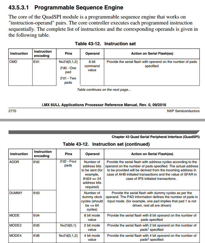
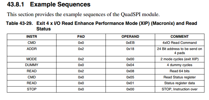
1. reference IMX6ULLRM.pdf:
Table 8-23. QuadSPI configuration parameters
43.5.3.1 Programmable Sequence Engine
43.8.1 Example Sequences
2. my worked configure file:
0 /*dqs_loopback=0 or 1*/
0 /*hold_delay=0 to 3*/
0 /*hsphs=0 (Half Speed Phase sampling at non-inverted clock) or 1 (sampling at inverted clock)*/
0 /*hsdly=0 (Half Speed Delay one clk delay) or 1 (two clk cycle delay)*/
0 /*device_quad_mode_en=1 to enable sending command to SPI device*/
0 /*device_cmd=command to device for enableing Quad I/O mode*/
0 /*write_cmd_ipcr=hex value to be written to IPCR register for write cmd of device*/
2000000 /*write_enable_ipcr=hex value to be written to IPCR register for write enable of device*/
3 /*cs_hold_time=0 to 0xF*/
3 /*cs_setup_time=0 to 0xF*/
8000000 /*sflash_A1_size=size in byte(hex)*/
0 /*sflash_A2_size=size in byte(hex)*/
8000000 /*sflash_B1_size=size in byte(hex)*/
0 /*sflash_B2_size=size in byte(hex)*/
1 /*sclk_freq=0 to 6*/
0 /*busy_bit_offset=bit position of device BUSY in device status register*/
1 /*sflash_type=1 (Single), 2 (Dual), 4 (Quad mode of operation)*/
0 /*sflash_port=0 or 1 (Port B used)*/
0 /*ddr_mode_enable=0 or 1*/
0 /*dqs_enable=0 or 1*/
0 /*parallel_mode_enable=0 or 1*/
0 /*portA_cs1=0 or 1*/
0 /*portB_cs1=0 or 1*/
0 /*fsphs=0 (Full Speed Phase sampling at non-inverted clock) or 1 (sampling at inverted clock)*/
0 /*fsdly=0 (Full Speed Delay One clk delay) or 1 (two clk cycle delay)*/
0 /*ddrsmp=0 to 7 (sampling point for incoming data in DDR mode)*/
08180403 /*lut[0] command sequence*/
24001c08 /*lut[1] command sequence*/
0 /*lut[2] command sequence*/
0 /*lut[3] command sequence*/
0 /*lut[4] command sequence*/
0 /*lut[5] command sequence*/
0 /*lut[6] command sequence*/
0 /*lut[7] command sequence*/
0 /*lut[8] command sequence*/
0 /*lut[9] command sequence*/
0 /*lut[10] command sequence*/
0 /*lut[11] command sequence*/
0 /*lut[12] command sequence*/
0 /*lut[13] command sequence*/
0 /*lut[14] command sequence*/
0 /*lut[15] command sequence*/
0 /*lut[16] command sequence*/
0 /*lut[17] command sequence*/
0 /*lut[18] command sequence*/
0 /*lut[19] command sequence*/
0 /*lut[20] command sequence*/
0 /*lut[21] command sequence*/
0 /*lut[22] command sequence*/
0 /*lut[23] command sequence*/
0 /*lut[24] command sequence*/
0 /*lut[25] command sequence*/
0 /*lut[26] command sequence*/
0 /*lut[27] command sequence*/
0 /*lut[28] command sequence*/
0 /*lut[29] command sequence*/
0 /*lut[30] command sequence*/
0 /*lut[31] command sequence*/
0 /*lut[32] command sequence*/
0 /*lut[33] command sequence*/
0 /*lut[34] command sequence*/
0 /*lut[35] command sequence*/
0 /*lut[36] command sequence*/
0 /*lut[37] command sequence*/
0 /*lut[38] command sequence*/
0 /*lut[39] command sequence*/
0 /*lut[40] command sequence*/
0 /*lut[41] command sequence*/
0 /*lut[42] command sequence*/
0 /*lut[43] command sequence*/
0 /*lut[44] command sequence*/
0 /*lut[45] command sequence*/
0 /*lut[46] command sequence*/
0 /*lut[47] command sequence*/
0 /*lut[48] command sequence*/
0 /*lut[49] command sequence*/
0 /*lut[50] command sequence*/
0 /*lut[51] command sequence*/
0 /*lut[52] command sequence*/
0 /*lut[53] command sequence*/
0 /*lut[54] command sequence*/
0 /*lut[55] command sequence*/
0 /*lut[56] command sequence*/
0 /*lut[57] command sequence*/
0 /*lut[58] command sequence*/
0 /*lut[59] command sequence*/
0 /*lut[60] command sequence*/
0 /*lut[61] command sequence*/
0 /*lut[62] command sequence*/
0 /*lut[63] command sequence*/
1000001 /*read_status_ipcr=hex value to be written to IPCR register for reading status reg of device*/
0 /*enable_dqs_phase=0 or 1*/
0 /*config_cmds_en, enable config command*/
0 /*config_cmds[0]*/
0 /*config_cmds[1]*/
0 /*config_cmds[2]*/
0 /*config_cmds[3]*/
0 /*config_cmds_args[0]*/
0 /*config_cmds_args[1]*/
0 /*config_cmds_args[2]*/
0 /*config_cmds_args[3]*/
0 /*io_pad_override_setting QSPI pins override setting*/
0 /*reserve[0], 25 byte reserved area*/
0 /*reserve[1], 25 byte reserved area*/
0 /*reserve[2], 25 byte reserved area*/
0 /*reserve[3], 25 byte reserved area*/
0 /*reserve[4], 25 byte reserved area*/
0 /*reserve[5], 25 byte reserved area*/
0 /*reserve[6], 25 byte reserved area*/
0 /*reserve[7], 25 byte reserved area*/
0 /*reserve[8], 25 byte reserved area*/
0 /*reserve[9], 25 byte reserved area*/
0 /*reserve[10], 25 byte reserved area*/
0 /*reserve[11], 25 byte reserved area*/
0 /*reserve[12], 25 byte reserved area*/
0 /*reserve[13], 25 byte reserved area*/
0 /*reserve[14], 25 byte reserved area*/
0 /*reserve[15], 25 byte reserved area*/
0 /*reserve[16], 25 byte reserved area*/
0 /*reserve[17], 25 byte reserved area*/
0 /*reserve[18], 25 byte reserved area*/
0 /*reserve[19], 25 byte reserved area*/
0 /*reserve[20], 25 byte reserved area*/
0 /*reserve[21], 25 byte reserved area*/
0 /*reserve[22], 25 byte reserved area*/
0 /*reserve[23], 25 byte reserved area*/
0 /*reserve[24], 25 byte reserved area*/
c0ffee01 /*tag, QSPI configuration tag, should be 0xc0ffee01*/
- Mark as New
- Bookmark
- Subscribe
- Mute
- Subscribe to RSS Feed
- Permalink
- Report Inappropriate Content
Hi jianlei
please refer to Table 8-23. QuadSPI Configuration Parameters
i.MX6UL Reference Manual
http://www.nxp.com/docs/en/reference-manual/IMX6ULRM.pdf
Best regards
igor
-----------------------------------------------------------------------------------------------------------------------
Note: If this post answers your question, please click the Correct Answer button. Thank you!
-----------------------------------------------------------------------------------------------------------------------

