- Forums
- Product Forums
- General Purpose MicrocontrollersGeneral Purpose Microcontrollers
- i.MX Forumsi.MX Forums
- QorIQ Processing PlatformsQorIQ Processing Platforms
- Identification and SecurityIdentification and Security
- Power ManagementPower Management
- Wireless ConnectivityWireless Connectivity
- RFID / NFCRFID / NFC
- MCX Microcontrollers
- S32G
- S32K
- S32V
- MPC5xxx
- Other NXP Products
- S12 / MagniV Microcontrollers
- Powertrain and Electrification Analog Drivers
- Sensors
- Vybrid Processors
- Digital Signal Controllers
- 8-bit Microcontrollers
- ColdFire/68K Microcontrollers and Processors
- PowerQUICC Processors
- OSBDM and TBDML
- S32M
-
- Solution Forums
- Software Forums
- MCUXpresso Software and ToolsMCUXpresso Software and Tools
- CodeWarriorCodeWarrior
- MQX Software SolutionsMQX Software Solutions
- Model-Based Design Toolbox (MBDT)Model-Based Design Toolbox (MBDT)
- FreeMASTER
- eIQ Machine Learning Software
- Embedded Software and Tools Clinic
- S32 SDK
- S32 Design Studio
- GUI Guider
- Zephyr Project
- Voice Technology
- Application Software Packs
- Secure Provisioning SDK (SPSDK)
- Processor Expert Software
-
- Topics
- Mobile Robotics - Drones and RoversMobile Robotics - Drones and Rovers
- NXP Training ContentNXP Training Content
- University ProgramsUniversity Programs
- Rapid IoT
- NXP Designs
- SafeAssure-Community
- OSS Security & Maintenance
- Using Our Community
-
- Cloud Lab Forums
-
- Knowledge Bases
- ARM Microcontrollers
- i.MX Processors
- Identification and Security
- Model-Based Design Toolbox (MBDT)
- QorIQ Processing Platforms
- S32 Automotive Processing Platform
- Wireless Connectivity
- CodeWarrior
- MCUXpresso Suite of Software and Tools
- MQX Software Solutions
-
- Home
- :
- i.MX フォーラム
- :
- i.MXプロセッサ
- :
- PCIe clock suggestion
PCIe clock suggestion
- RSS フィードを購読する
- トピックを新着としてマーク
- トピックを既読としてマーク
- このトピックを現在のユーザーにフロートします
- ブックマーク
- 購読
- ミュート
- 印刷用ページ
PCIe clock suggestion
- 新着としてマーク
- ブックマーク
- 購読
- ミュート
- RSS フィードを購読する
- ハイライト
- 印刷
- 不適切なコンテンツを報告
Hi All,
It seems that many people are facing issue about the PCIe on platform based on IMX6.
I plan to interface a PCIe device (EP) to an iMX6 CPU (RC) and i noticed on several schematics that the PCIe clock was often driven by the diff output CLK1_P/N (LVDS vs HCSL for PCIe) or an external PCIe clock generator.
Could you please tell me the recommendations about this point ?
If i use the CLK1_P/N diff output as PCIe ref clock, could you please tell me how to translate LVDS to HCSL ?
BR,
Greg
- 新着としてマーク
- ブックマーク
- 購読
- ミュート
- RSS フィードを購読する
- ハイライト
- 印刷
- 不適切なコンテンツを報告
The CLKx_P/N differential clock outputs can be used directly as a reference clock source for the PCIe bus. For example, the i.MX6Q SABRE SD board implements it this way, look at its schematic for the reference. The schematic is available as the part of the i.MX6_SABRE_SDP_DESIGNFILES package on the NXP web site (check the "Schematics" section):
Have a great day,
Artur
-----------------------------------------------------------------------------------------------------------------------
Note: If this post answers your question, please click the Correct Answer button. Thank you!
-----------------------------------------------------------------------------------------------------------------------
- 新着としてマーク
- ブックマーク
- 購読
- ミュート
- RSS フィードを購読する
- ハイライト
- 印刷
- 不適切なコンテンツを報告
Artur,
Thanks for your reply.
I found in the HW Design Checking List for i.Mx6DQSDL Rev3.0.xlsx an answer.
BTW, this document is not very easy to download.
Anyway here is my understanding
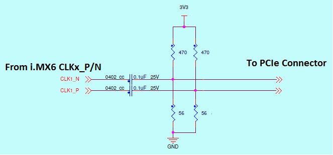
If i don't need to be compliant to GEN2 i can use a low cost solution describe below:
Due to CLKx_P/N is LVDS port and don't match with PCIe reference clock specification. For PCIe Gen1 application, following low cost soultion can be used(DC bias and AC impedance should be considered).
----------------------------------------------------------------------------------------------------------------------------------------------------------------------------------------------------
If i want to be compliant to GEN2, i need to implement the solution below:
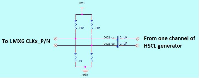
PCIe reference clock solution which provided by CLKx_N/P of i.MX6 chip can't pass PCIe Gen2 compliance test. Recommend using external PCIe 2.0/3.0 clock generator with 2 HCSL outputs solution. One clock channel connect to i.MX6 as a reference input, please click Ref14 for reference circuit. Another clock channel should connect to PCIe connector, please contact generator vendor for detailed design guide.
Just one question:
If i use a GEN2 Endpoint device does it mean that the low cost solution is not functional ?
- 新着としてマーク
- ブックマーク
- 購読
- ミュート
- RSS フィードを購読する
- ハイライト
- 印刷
- 不適切なコンテンツを報告
First, please refer to officially published i.MX6 series Hardware Development Guide document, that can be found on the NXP web site (check the "Users Guides" section):
i.MX6Q|i.MX 6Quad Processors|Quad Core|NXP
The document you mentioned is not officially verified.
The solution that uses the CLKx_P/N signals is functional for both Gen1 and Gen.2. The i.MX6 SABRE AI board that implements this solution has passed the PCIe sertification test, please refer to the AN4784 App Note document, available on the same web page.
Have a great day,
Artur

