- Forums
- Product Forums
- General Purpose MicrocontrollersGeneral Purpose Microcontrollers
- i.MX Forumsi.MX Forums
- QorIQ Processing PlatformsQorIQ Processing Platforms
- Identification and SecurityIdentification and Security
- Power ManagementPower Management
- Wireless ConnectivityWireless Connectivity
- RFID / NFCRFID / NFC
- MCX Microcontrollers
- S32G
- S32K
- S32V
- MPC5xxx
- Other NXP Products
- S12 / MagniV Microcontrollers
- Powertrain and Electrification Analog Drivers
- Sensors
- Vybrid Processors
- Digital Signal Controllers
- 8-bit Microcontrollers
- ColdFire/68K Microcontrollers and Processors
- PowerQUICC Processors
- OSBDM and TBDML
- S32M
-
- Solution Forums
- Software Forums
- MCUXpresso Software and ToolsMCUXpresso Software and Tools
- CodeWarriorCodeWarrior
- MQX Software SolutionsMQX Software Solutions
- Model-Based Design Toolbox (MBDT)Model-Based Design Toolbox (MBDT)
- FreeMASTER
- eIQ Machine Learning Software
- Embedded Software and Tools Clinic
- S32 SDK
- S32 Design Studio
- GUI Guider
- Zephyr Project
- Voice Technology
- Application Software Packs
- Secure Provisioning SDK (SPSDK)
- Processor Expert Software
-
- Topics
- Mobile Robotics - Drones and RoversMobile Robotics - Drones and Rovers
- NXP Training ContentNXP Training Content
- University ProgramsUniversity Programs
- Rapid IoT
- NXP Designs
- SafeAssure-Community
- OSS Security & Maintenance
- Using Our Community
-
- Cloud Lab Forums
-
- Knowledge Bases
- ARM Microcontrollers
- i.MX Processors
- Identification and Security
- Model-Based Design Toolbox (MBDT)
- QorIQ Processing Platforms
- S32 Automotive Processing Platform
- Wireless Connectivity
- CodeWarrior
- MCUXpresso Suite of Software and Tools
- MQX Software Solutions
-
- Home
- :
- i.MX フォーラム
- :
- i.MXプロセッサ
- :
- Re: How to calibrate DDR4 on i.MX8M-nano with i.MX/Mscale DDR Tool?
How to calibrate DDR4 on i.MX8M-nano with i.MX/Mscale DDR Tool?
- RSS フィードを購読する
- トピックを新着としてマーク
- トピックを既読としてマーク
- このトピックを現在のユーザーにフロートします
- ブックマーク
- 購読
- ミュート
- 印刷用ページ
- 新着としてマーク
- ブックマーク
- 購読
- ミュート
- RSS フィードを購読する
- ハイライト
- 印刷
- 不適切なコンテンツを報告
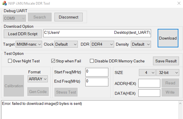
Using the provided guides, the following error occurs, while using Mscale DDR Tool:
"Error: failed to download image(0 bytes is sent)"
- i.MX8 MSCALE SERIES DDR Tool Release (V3.10)
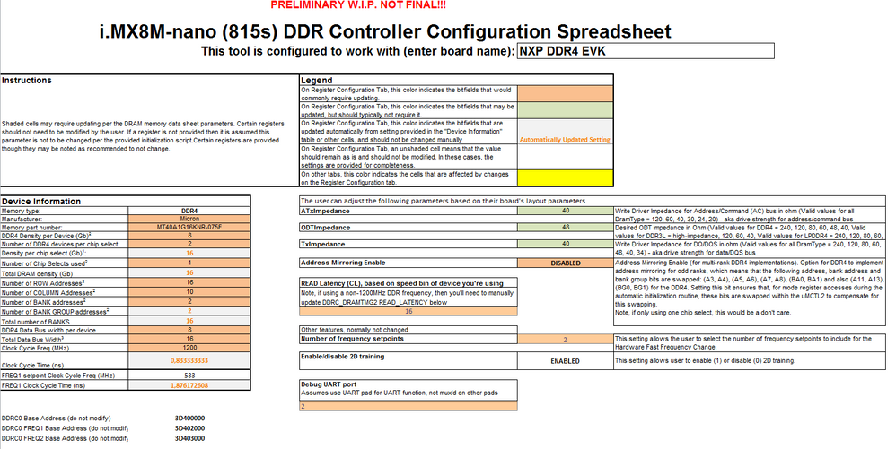
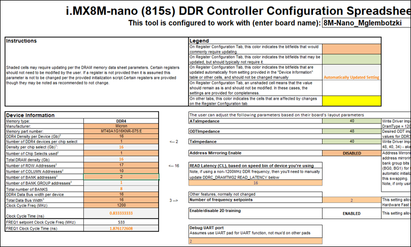
Could you please verify the configuration is right? I would expect the Number of Bank Group addresses is 2, but the field is not editable.
Further infos:
- custom board using i.MX8M-nano
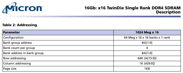
- DDR4: MT40A1G16KNR-075:E (please see addressing table below)
- PMIC: BD71847AMWV-E2 (not quiete sure, if you need this info)
- UART1
解決済! 解決策の投稿を見る。
- 新着としてマーク
- ブックマーク
- 購読
- ミュート
- RSS フィードを購読する
- ハイライト
- 印刷
- 不適切なコンテンツを報告
Hello Michael,
this is just to finish this thread, even if the solution already reached you on a different channel:
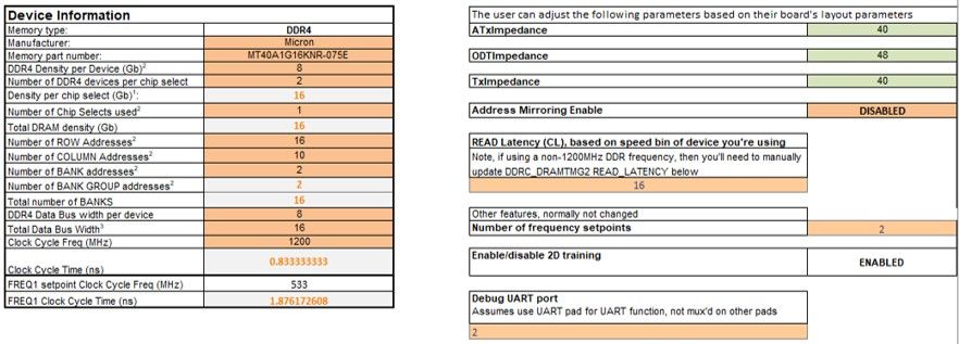
Using 8M Nano with the twin-die device MT40A1G16-KNR-075E requires the following settings in the RPA tool:
On top of the correct configuration it is also important to use a new version of the RPA file (attached), in previous versions
there is a bug in the DDRC settings for such kind of memory configuration.
Regards,
Bernhard.
- 新着としてマーク
- ブックマーク
- 購読
- ミュート
- RSS フィードを購読する
- ハイライト
- 印刷
- 不適切なコンテンツを報告
I have the same problem. We have a custom board that is basically a copy of the i.mx8m mini evk. Neither the EVK nor our custom board will work and we get the same result as the OP.
Set dip switch W1101to 1010xxxxxx and SW1102 to xxxxxxxxx0. Power up board, tried both COM ports discovered, select the imx8 mini script and hit download and nothing but error message.
Repeat the same steps on our custom board and get same result. Try different Windows machine ... same result.
No clue what I'm doing wrong but I would expect using the provided script for the evk should just work.
Regards,
Brian
- 新着としてマーク
- ブックマーク
- 購読
- ミュート
- RSS フィードを購読する
- ハイライト
- 印刷
- 不適切なコンテンツを報告
Hello Bernhard,
thanks for the reply. We have only an eMMC (no SD card) on our PCB. Also the USB Connection is ok. I verified the setup with the imx8mn-evk.
Any other suggestions?
Best Michael
- 新着としてマーク
- ブックマーク
- 購読
- ミュート
- RSS フィードを購読する
- ハイライト
- 印刷
- 不適切なコンテンツを報告
Hello,
Please check if the board is working, using sections 2 (i.MX 8M Nano design checklist)
and 4 (Avoiding board bring-up problems) of i.MX 8M Nano Hardware Developer’s Guide.
https://www.nxp.com/docs/en/user-guide/IMX8MNHDG.pdf
Have a great day,
Yuri.
-------------------------------------------------------------------------------
Note:
- If this post answers your question, please click the "Mark Correct" button. Thank you!
- We are following threads for 7 weeks after the last post, later replies are ignored
Please open a new thread and refer to the closed one, if you have a related question at a later point in time.
- 新着としてマーク
- ブックマーク
- 購読
- ミュート
- RSS フィードを購読する
- ハイライト
- 印刷
- 不適切なコンテンツを報告
Ok, so the GUI works fine with an 8M Nano EVK, so it has nothing to do with the GUI setup.
What's left over is your custom 8MN board.
As Yuri wrote, can you prove that your board boots correctly? Do you have a JTAG debugger for a crosscheck?
Regards,
Bernhard.
- 新着としてマーク
- ブックマーク
- 購読
- ミュート
- RSS フィードを購読する
- ハイライト
- 印刷
- 不適切なコンテンツを報告
Thanks for the reply.
Please check if the board is working, using sections 2 (i.MX 8M Nano design checklist)
and 4 (Avoiding board bring-up problems) of i.MX 8M Nano Hardware Developer’s Guide.
We double checked and could not find any open issue.
The same behaviour occurs, when trying to boot u-boot from the bootable image. The u-boot-spl boots until the romapi comes into place.
g_rom_api->download_image(p, 0, pg, ((uintptr_t)p)^pg); # from spl_imx_romapi.c (rel_imx_4.14.98_2.3.0)
The hole RAM is empty (=zero), after executing download_image. And this is the same error, we prior saw in mscale tool (Error failed to download image). Nevertheless reading/writing onto the RAM is working without ROMAPI. Do you have any ideas, what to check next?
Here the u-boot-spl log.
U-Boot SPL 2018.03-01269-gdb543bb8f4-dirty (Feb 10 2020 - 13:13:19 +0100)
DDRINFO: start DRAM init
[..]
Normal Boot
Trying to boot from ROMAPI
First loop done
Can't found uboot FIT image in 640K range
SPL: failed to boot from all boot devices
### ERROR ### Please RESET the board ###
- 新着としてマーク
- ブックマーク
- 購読
- ミュート
- RSS フィードを購読する
- ハイライト
- 印刷
- 不適切なコンテンツを報告
Hi Bernhard, hi Yuri,
using a native Windows machine solved the download image error. Now mscale works as espected and the connection can be established. We modified the RPA, but after download the following error occurs, when accessing the DDR memory.
Download is complete
Waiting for the target board boot...===================hardware_init=====================
PMIC is initialized in DDR script
Write 0x1 to PMIC reg[0x2f] successfully
Write 0x14 to PMIC reg[0xd] successfully
Write 0x28 to PMIC reg[0x17] successfully
Write 0xf to PMIC reg[0xf] successfully
Write 0x11 to PMIC reg[0x2f] successfully
hardware_init exit*************************************************************************
*************************************************************************
*************************************************************************
MX8 DDR Stress Test V3.10
Built on Feb 5 2020 13:02:45
*************************************************************************--Set up the MMU and enable I and D cache--
- This is the Cortex-A53 core
- Check if I cache is enabled
- Enabling I cache since it was disabled
- Push base address of TTB to TTBR0_EL3
- Config TCR_EL3
- Config MAIR_EL3
- Enable MMU
- Data Cache has been enabled
- Check system memory register, only for debug- VMCR Check:
- ttbr0_el3: 0x97d000
- tcr_el3: 0x2051c
- mair_el3: 0x774400
- sctlr_el3: 0xc01815
- id_aa64mmfr0_el1: 0x1122- MMU and cache setup complete
*************************************************************************
ARM clock(CA53) rate: 1500MHz
DDR Clock: 1200MHz============================================
DDR configuration
DDR type is DDR4
Data width: 16, bank num: 16
For DDR4, bank num is the total of 4 bank groups and 4 banks per group
Row size: 16, col size: 10
One chip select is used
Number of DDR controllers used on the SoC: 1
Density per chip select: 2048MB
Density per controller is: 2048MB
Total density detected on the board is: 2048MB
============================================MX8M-nano: Cortex-A53 is found
*************************************************************************
============ Step 1: DDRPHY Training... ============
---DDR 1D-Training @1200Mhz...
[Process] End of initialization
[Process] End of read enable training
[Process] End of fine write leveling
[Process] End of read DQ deskew training
[Process] End of MPR read delay center optimization
[Process] End of Write Leveling coarse delay
[Process] End of write delay center optimization
[Process] End of read delay center optimization
[Process] End of max read latency training
[Result] PASS
---DDR 1D-Training @533Mhz...
[Process] End of initialization
[Process] End of read enable training
[Process] End of fine write leveling
[Process] End of MPR read delay center optimization
[Process] End of Write Leveling coarse delay
[Process] End of write delay center optimization
[Process] End of read delay center optimization
[Process] End of max read latency training
[Result] PASS
---DDR 2D-Training @1200Mhz...
[Process] End of initialization
[Process] End of 2D read delay/voltage center optimization
[Process] End of 2D write delay/voltage center optimization
[Result] PASS============ Step 2: DDR memory accessing... ============
Verifying DDR frequency point0@1200MHz......Address of failure: 0x0000000040080000
Data read was: 0x0000000040001000
But pattern was: 0x0000000040000000
Failed
Please modify DDRC/DFI parameters!!!
- 新着としてマーク
- ブックマーク
- 購読
- ミュート
- RSS フィードを購読する
- ハイライト
- 印刷
- 不適切なコンテンツを報告
Hi bernhardfink, hi Yuri,
could you please check my RPA (xlsx) configuration attached in the original question?
Best,
Michael
- 新着としてマーク
- ブックマーク
- 購読
- ミュート
- RSS フィードを購読する
- ハイライト
- 印刷
- 不適切なコンテンツを報告
Hi Michael,
this is the memory you use: https://www.micron.com/-/media/client/global/documents/products/data-sheet/dram/ddr4/ddr4_16gb_x16_1...
This is the memory we have on the 8M-Nano EVK: https://www.micron.com/-/media/client/global/documents/products/data-sheet/dram/ddr4/16gb_ddr4_sdram...
You have a twin-die device: "The 16Gb (TwinDie™) DDR4 SDRAM uses Micron’s 8Gb DDR4 SDRAM die; two x8s combined to make one x16."
We have a single die device.
So there are a few differences which you need to take into account in the Excel file, see below my proposal:
Regards,
Bernhard.
- 新着としてマーク
- ブックマーク
- 購読
- ミュート
- RSS フィードを購読する
- ハイライト
- 印刷
- 不適切なコンテンツを報告
Thanks for the reply bernhardfink,
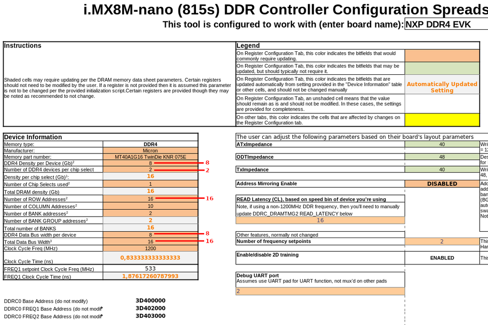
- 新着としてマーク
- ブックマーク
- 購読
- ミュート
- RSS フィードを購読する
- ハイライト
- 印刷
- 不適切なコンテンツを報告
Hi Michael,
I will crosscheck your settings with an expert, but it seems you are right with these two settings:
This parameter controls DDR training debug message. The default value is 0xc8, which means only display stage completion message. You can change to 0x05 to get detailed debug message when DDR training failed.
- ODTImpedance
Desired ODT impedance in Ohm. Valid values for DDR4=240,120,80,60,40. Valid values for
DDR3L=high-impedance,120,60,40. Valid values for LPDDR4=240,120,80,60,40
- TxImpedance
Write Driver Impedance for DQ/DQS in ohm (Valid values for all DDR type= 240, 120, 80, 60, 48, 40, 34)
- ATxImpedance
Write Driver Impedance for Address/Command (AC) bus in Ohm (Valid values for all DDR type = 120, 60, 40, 30, 24, 20)
But pattern was: 0x0000000040000000
- 新着としてマーク
- ブックマーク
- 購読
- ミュート
- RSS フィードを購読する
- ハイライト
- 印刷
- 不適切なコンテンツを報告
Hello Michael,
this is just to finish this thread, even if the solution already reached you on a different channel:
Using 8M Nano with the twin-die device MT40A1G16-KNR-075E requires the following settings in the RPA tool:
On top of the correct configuration it is also important to use a new version of the RPA file (attached), in previous versions
there is a bug in the DDRC settings for such kind of memory configuration.
Regards,
Bernhard.
- 新着としてマーク
- ブックマーク
- 購読
- ミュート
- RSS フィードを購読する
- ハイライト
- 印刷
- 不適切なコンテンツを報告
Hi @bernhardfink ,
we have the same issue on our i.MX8M Mini customer board,
============ Step 1: DDRPHY Training... ============
---DDR 1D-Training @1200Mhz...
[Process] End of initialization
[Process] End of read enable training
[Process] End of fine write leveling
[Process] End of read DQ deskew training
[Process] End of MPR read delay center optimization
[Process] End of Write Leveling coarse delay
[Process] End of write delay center optimization
[Process] End of read delay center optimization
[Process] End of max read latency training
[Result] PASS
---DDR 1D-Training @668Mhz...
[Process] End of initialization
[Process] End of read enable training
[Process] End of fine write leveling
[Process] End of MPR read delay center optimization
[Process] End of Write Leveling coarse delay
[Process] End of write delay center optimization
[Process] End of read delay center optimization
[Process] End of max read latency training
[Result] PASS
---DDR 2D-Training @1200Mhz...
[Process] End of initialization
[Process] End of 2D read delay/voltage center optimization
[Process] End of 2D write delay/voltage center optimization
[Result] PASS
============ Step 2: DDR memory accessing... ============
Verifying DDR frequency point0@1200MHz......Address of failure: 0x00000000400800D0
Data read was: 0x00000000400008C0
But pattern was: 0x00000000400000D0
Failed
Please modify DDRC/DFI parameters!!!
Will you please check the"MX8M_Mini_DDR4_RPA_v15.xlsx" ?
- 新着としてマーク
- ブックマーク
- 購読
- ミュート
- RSS フィードを購読する
- ハイライト
- 印刷
- 不適切なコンテンツを報告
Your settings seem to be correct, you connected one 8Gbit DDR4 and you use 16-bit memory bus width.
The error at 0x400800D0 looks more like a electrical performance problem than a configuration problem. 2 bits are flipped.
I want to bring a new tool to your attention, which may help with this. The "Config Tool for i.MX" in version 9 includes a more powerful DDR test tool:
https://www.nxp.com/webapp/Download?colCode=PINS-IMX-WIN64-V9&appType=license&location=null
https://www.nxp.com/webapp/Download?colCode=PINS-IMX-LINUX64-DEB-V9&appType=license&location=null
It works with the same hardware setup as the DDR Stress Test Tool, but provides more options. A very brief introduction is attached.
You could decrease the clock cycle frequency from 1200MHz to 800MHz for example, this is also helpful to find out whether there is a performance problem or a configuration problem.
Regards,
Bernhard.
- 新着としてマーク
- ブックマーク
- 購読
- ミュート
- RSS フィードを購読する
- ハイライト
- 印刷
- 不適切なコンテンツを報告
Hi @bernhardfink ,
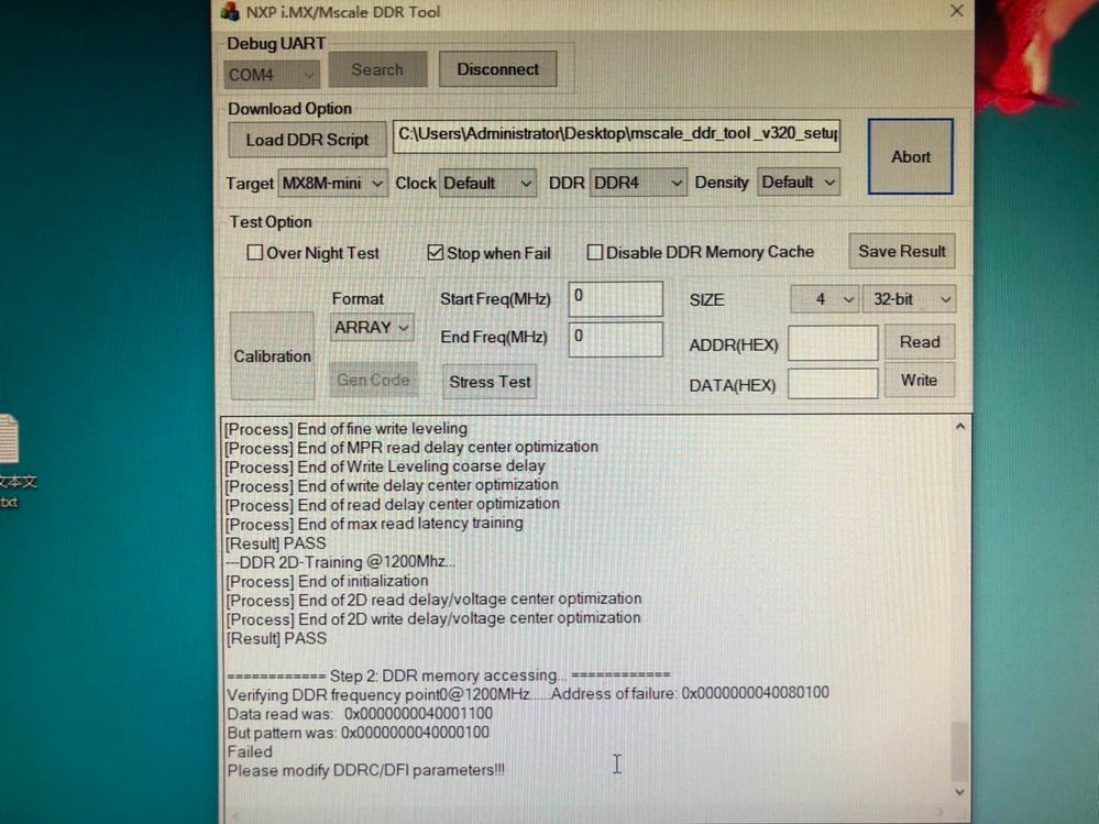
we have modified the value of ODTImpedance to 240,the error has only 1 bit flipped.
Verifying DDR frequency point0@1200MHz......Address of failure: 0x0000000040080000
Data read was: 0x0000000040001000
But pattern was: 0x0000000040000000
Failed
Please modify DDRC/DFI parameters!!!
Verifying DDR frequency point0@1200MHz......Address of failure: 0x00000000400800C0
Data read was: 0x00000000400010C0
But pattern was: 0x00000000400000C0
Failed
Please modify DDRC/DFI parameters!!!
- 新着としてマーク
- ブックマーク
- 購読
- ミュート
- RSS フィードを購読する
- ハイライト
- 印刷
- 不適切なコンテンツを報告
Hi @chao ,
with the new DDR test tool you can maybe identify the signal lines which are performing badly. If there are impedance mismatches in the line(s), then there is nothing more you could do in software, it requires a hardware change.
Regards,
Bernhard.
- 新着としてマーク
- ブックマーク
- 購読
- ミュート
- RSS フィードを購読する
- ハイライト
- 印刷
- 不適切なコンテンツを報告
Hi Brian,
this is most likely solved on your side already, I just want to finish this thread with some useful comments.
The USB connection to the chip can be tested as well with the UUU utility. If this works in some way, then you have at least verified the SDP (serial download protocol) functionality.
The DDR test GUI also uses the same USB SDP protocol to download a test firmware into the RAM of the i.MX and start it. The communication channel after the download is the UART .
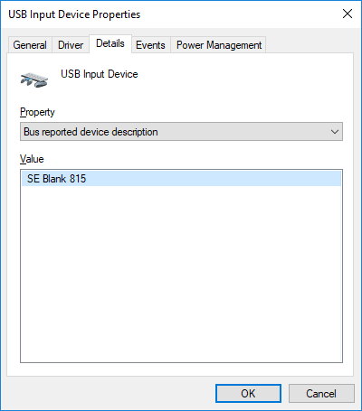
If you have an 8MM or 8MN in USB download mode, then on the Windows PC side you will get a new "USB Input Device" in the Device Manager, you can verify it by checking this: (shown for an 8M Nano)
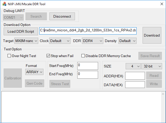
When you start the DDR Tool, it will ask for admin rights, then you need to make the following settings:
- select the second COM port in the list (for 8MM and 8MN EVK), on your own board of course the one you connected and at the same time specified in the Excel file
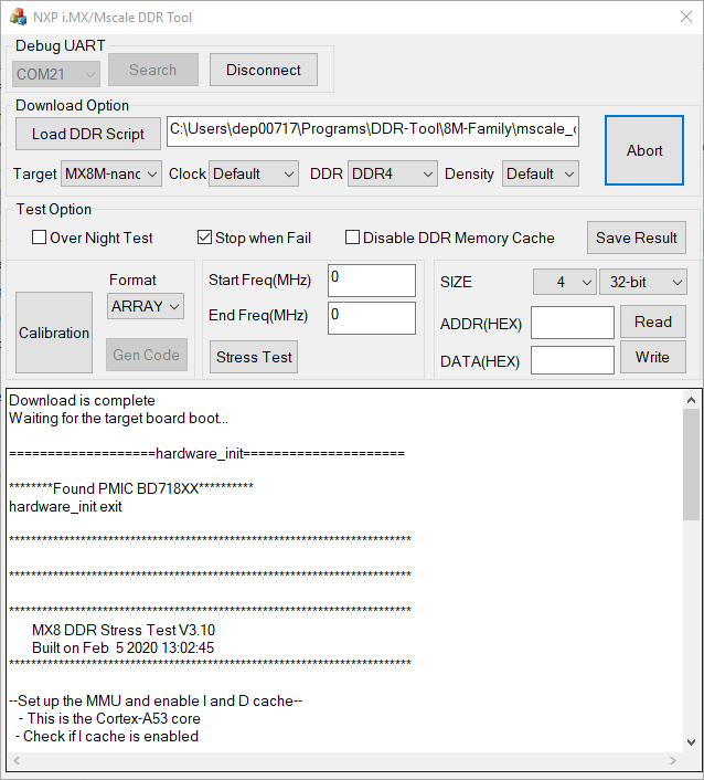
Just to be sure, make a fresh reset of the board and then click on Download, you must get the following:
Regards,
Bernhard.
- 新着としてマーク
- ブックマーク
- 購読
- ミュート
- RSS フィードを購読する
- ハイライト
- 印刷
- 不適切なコンテンツを報告
You stated "using a native Windows machine solved the download image error" and I asked you what you meant by "native Windows machine".
I'm having the exact same problem with not being able to download an image with the exact same tool you're posting about. I stated my concern about the documentation stating not using a "USB hub" and wondered if there was a difference using the tool with a laptop vs a desktop so was curious when you say "native Windows machine" what that means.
Curious that you think I'm spamming when I'm asking relevant questions about the tool and what you did different to get it to work when I'm having the same issues.
Regards,
Brian
- 新着としてマーク
- ブックマーク
- 購読
- ミュート
- RSS フィードを購読する
- ハイライト
- 印刷
- 不適切なコンテンツを報告
What do you mean about "native Windows machine"??? I saw the warning about not connecting using a USB hub ... which made me wonder since I was using a laptop. I thought about trying it on a desktop ... so curious what you mean by "native".
Regards,
Brian
- 新着としてマーク
- ブックマーク
- 購読
- ミュート
- RSS フィードを購読する
- ハイライト
- 印刷
- 不適切なコンテンツを報告
Hello,
As recommended for the tool users must run it in administrator mode.
Is it so in Your case?
Regards,
Yuri.
- 新着としてマーク
- ブックマーク
- 購読
- ミュート
- RSS フィードを購読する
- ハイライト
- 印刷
- 不適切なコンテンツを報告
