- Forums
- Product Forums
- General Purpose MicrocontrollersGeneral Purpose Microcontrollers
- i.MX Forumsi.MX Forums
- QorIQ Processing PlatformsQorIQ Processing Platforms
- Identification and SecurityIdentification and Security
- Power ManagementPower Management
- Wireless ConnectivityWireless Connectivity
- RFID / NFCRFID / NFC
- Advanced AnalogAdvanced Analog
- MCX Microcontrollers
- S32G
- S32K
- S32V
- MPC5xxx
- Other NXP Products
- S12 / MagniV Microcontrollers
- Powertrain and Electrification Analog Drivers
- Sensors
- Vybrid Processors
- Digital Signal Controllers
- 8-bit Microcontrollers
- ColdFire/68K Microcontrollers and Processors
- PowerQUICC Processors
- OSBDM and TBDML
- S32M
- S32Z/E
-
- Solution Forums
- Software Forums
- MCUXpresso Software and ToolsMCUXpresso Software and Tools
- CodeWarriorCodeWarrior
- MQX Software SolutionsMQX Software Solutions
- Model-Based Design Toolbox (MBDT)Model-Based Design Toolbox (MBDT)
- FreeMASTER
- eIQ Machine Learning Software
- Embedded Software and Tools Clinic
- S32 SDK
- S32 Design Studio
- GUI Guider
- Zephyr Project
- Voice Technology
- Application Software Packs
- Secure Provisioning SDK (SPSDK)
- Processor Expert Software
- Generative AI & LLMs
-
- Topics
- Mobile Robotics - Drones and RoversMobile Robotics - Drones and Rovers
- NXP Training ContentNXP Training Content
- University ProgramsUniversity Programs
- Rapid IoT
- NXP Designs
- SafeAssure-Community
- OSS Security & Maintenance
- Using Our Community
-
- Cloud Lab Forums
-
- Knowledge Bases
- ARM Microcontrollers
- i.MX Processors
- Identification and Security
- Model-Based Design Toolbox (MBDT)
- QorIQ Processing Platforms
- S32 Automotive Processing Platform
- Wireless Connectivity
- CodeWarrior
- MCUXpresso Suite of Software and Tools
- MQX Software Solutions
- RFID / NFC
- Advanced Analog
-
- NXP Tech Blogs
Failed during ddr calibration
@igorpadykov
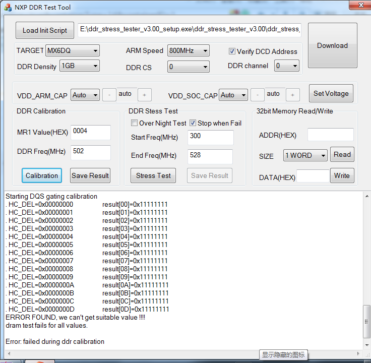
We are working our board with iMX6 Quad processor.,failed during ddr calibration when Freq greater than 500MHz,I use Stress Tool V3.0,thanks for the help in advance. The log is as below:
============================================
DDR Stress Test (3.0.0)
Build: Dec 14 2018, 14:12:06
NXP Semiconductors.
============================================
============================================
Chip ID
CHIP ID = i.MX6 Dual/Quad (0x63)
Internal Revision = TO1.5
============================================
============================================
Boot Configuration
SRC_SBMR1(0x020d8004) = 0x00000000
SRC_SBMR2(0x020d801c) = 0x00000001
============================================
ARM Clock set to 800MHz
============================================
DDR configuration
BOOT_CFG3[5-4]: 0x00, Single DDR channel.
DDR type is DDR3
Data width: 64, bank num: 8
Row size: 14, col size: 10
Chip select CSD0 is used
Density per chip select: 1024MB
============================================
Current Temperature: 63
============================================
DDR Freq: 528 MHz
ddr_mr1=0x00000004
Start write leveling calibration...
running Write level HW calibration
MPWLHWERR register read out for factory diagnostics:
MPWLHWERR PHY0 = 0x3e1f1f1f
MPWLHWERR PHY1 = 0x1f1f1f1f
Write leveling calibration completed, update the following registers in your initialization script
MMDC_MPWLDECTRL0 ch0 (0x021b080c) = 0x00000000
MMDC_MPWLDECTRL1 ch0 (0x021b0810) = 0x00050000
MMDC_MPWLDECTRL0 ch1 (0x021b480c) = 0x00000000
MMDC_MPWLDECTRL1 ch1 (0x021b4810) = 0x00000000
Write DQS delay result:
Write DQS0 delay: 0/256 CK
Write DQS1 delay: 0/256 CK
Write DQS2 delay: 0/256 CK
Write DQS3 delay: 5/256 CK
Write DQS4 delay: 0/256 CK
Write DQS5 delay: 0/256 CK
Write DQS6 delay: 0/256 CK
Write DQS7 delay: 0/256 CK
Starting DQS gating calibration
. HC_DEL=0x00000000 result[00]=0x11111111
. HC_DEL=0x00000001 result[01]=0x11111111
. HC_DEL=0x00000002 result[02]=0x11111111
. HC_DEL=0x00000003 result[03]=0x11111111
. HC_DEL=0x00000004 result[04]=0x11111111
. HC_DEL=0x00000005 result[05]=0x11111111
. HC_DEL=0x00000006 result[06]=0x11111111
. HC_DEL=0x00000007 result[07]=0x11111111
. HC_DEL=0x00000008 result[08]=0x11111111
. HC_DEL=0x00000009 result[09]=0x11111111
. HC_DEL=0x0000000A result[0A]=0x11111111
. HC_DEL=0x0000000B result[0B]=0x11111111
. HC_DEL=0x0000000C result[0C]=0x11111111
. HC_DEL=0x0000000D result[0D]=0x11111111
ERROR FOUND, we can't get suitable value !!!!
dram test fails for all values.
Error: failed during ddr calibration
Hi 江 涛
if erross are only for DQS gating calibration (all other tests passed),
they can be ignored. As common advice one can try to increase drive
strength and try test at lower frequencies. Recheck board layout against
sect.3.5 DDR routing rules i.MX6Q Hardware Guide
(so transmission path of some of the Byte Lanes is so long that maybe the DQS Gate
calibration routine of the Stress Test can't find find a suitable endpoint)
https://www.nxp.com/webapp/Download?colCode=IMX6DQ6SDLHDG
Best regards
igor
-----------------------------------------------------------------------------------------------------------------------
Note: If this post answers your question, please click the Correct Answer button. Thank you!
-----------------------------------------------------------------------------------------------------------------------
yes it can be due to layout or schematic, one can recheck
it using i.MX6Q Hardware Guide. Also one can test with jtag:
perform write/read from memory.
Best regards
igor
I use ddr3 stress tool V3.0 to test the development board that I buy,when I am going to do stress test,it also happens stress test fail,I am not sure that whether the ddr register configuration is wrong or I operate incorrectly? Thanks for your support
one can look at ddr test description in presentation:
DES-N1936 i.MX 6UltraLite DDR Tools Overview and Hardware Design Considerations
Best regards
igor
