- Forums
- Product Forums
- General Purpose MicrocontrollersGeneral Purpose Microcontrollers
- i.MX Forumsi.MX Forums
- QorIQ Processing PlatformsQorIQ Processing Platforms
- Identification and SecurityIdentification and Security
- Power ManagementPower Management
- Wireless ConnectivityWireless Connectivity
- RFID / NFCRFID / NFC
- Advanced AnalogAdvanced Analog
- MCX Microcontrollers
- S32G
- S32K
- S32V
- MPC5xxx
- Other NXP Products
- S12 / MagniV Microcontrollers
- Powertrain and Electrification Analog Drivers
- Sensors
- Vybrid Processors
- Digital Signal Controllers
- 8-bit Microcontrollers
- ColdFire/68K Microcontrollers and Processors
- PowerQUICC Processors
- OSBDM and TBDML
- S32M
- S32Z/E
-
- Solution Forums
- Software Forums
- MCUXpresso Software and ToolsMCUXpresso Software and Tools
- CodeWarriorCodeWarrior
- MQX Software SolutionsMQX Software Solutions
- Model-Based Design Toolbox (MBDT)Model-Based Design Toolbox (MBDT)
- FreeMASTER
- eIQ Machine Learning Software
- Embedded Software and Tools Clinic
- S32 SDK
- S32 Design Studio
- GUI Guider
- Zephyr Project
- Voice Technology
- Application Software Packs
- Secure Provisioning SDK (SPSDK)
- Processor Expert Software
- Generative AI & LLMs
-
- Topics
- Mobile Robotics - Drones and RoversMobile Robotics - Drones and Rovers
- NXP Training ContentNXP Training Content
- University ProgramsUniversity Programs
- Rapid IoT
- NXP Designs
- SafeAssure-Community
- OSS Security & Maintenance
- Using Our Community
-
- Cloud Lab Forums
-
- Knowledge Bases
- ARM Microcontrollers
- i.MX Processors
- Identification and Security
- Model-Based Design Toolbox (MBDT)
- QorIQ Processing Platforms
- S32 Automotive Processing Platform
- Wireless Connectivity
- CodeWarrior
- MCUXpresso Suite of Software and Tools
- MQX Software Solutions
- RFID / NFC
- Advanced Analog
-
- NXP Tech Blogs
- Home
- :
- i.MX フォーラム
- :
- i.MXプロセッサ
- :
- Changing I2C Configuration
Changing I2C Configuration
- RSS フィードを購読する
- トピックを新着としてマーク
- トピックを既読としてマーク
- このトピックを現在のユーザーにフロートします
- ブックマーク
- 購読
- ミュート
- 印刷用ページ
Changing I2C Configuration
- 新着としてマーク
- ブックマーク
- 購読
- ミュート
- RSS フィードを購読する
- ハイライト
- 印刷
- 不適切なコンテンツを報告
I'd like to change I2C voltage on DVP port. I have checked device tree for some hints but all I can find is this:
DOVDD-supply = <&vgen4_reg>; /* 1.8v */
AVDD-supply = <&vgen3_reg>; /* 2.8v, on rev C board is VGEN3,
on rev B board is VGEN5 */
DVDD-supply = <&vgen2_reg>; /* 1.5v*/
pwn-gpios = <&gpio1 16 1>; /* active low: SD1_DAT0 */
rst-gpios = <&gpio1 17 0>; /* active high: SD1_DAT1 */
There is no information about any of the *-supply variables.I can understand AVDD stands for analog VDD and DVDD stands for digital VDD but still it's not really clear.
Are they(DOVDD, AVDD, DVDD supply) for CSI-DVP configuration?
Can they also control I2C voltages?
Are I2C settings fixed, and not changeable?
- 新着としてマーク
- ブックマーク
- 購読
- ミュート
- RSS フィードを購読する
- ハイライト
- 印刷
- 不適切なコンテンツを報告
Hi mert can ergun,
My understanding is that you want to change the I2C operation voltage of the DVP (camera connector). Is this correct? So, in this case it would be necessary to modify HW rather than SW.
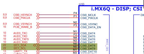
In SABRE board design, you can find that the I2C master signal comes from CSIO_DAT8 -> I2C1_SDA and CSIO_DAT9 -> I2C1_SCL pins on IMX6Q.
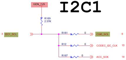
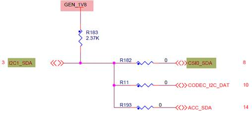
I2C1_SCL is connected to CSIO_SCL and I2C1_SDA is connected to CSIO_SDA, and both are connected with a pull-up to GEN_1V8
Then CSIO_SCL y CSIO_SDA is connected to J9 which is the camera connector for DVP.
Now, changing the I2C voltage could be done in different ways:
OPTION 1:
Change pull-ups, instead of “GEN_1V8” they may be connected to a power rail with the required voltage. Please note that in this case all the devices connected to this rail must support the same voltage, otherwise you may use option 3.
OPTION2:
You may also change voltage in VGEN4 on PF0100 (which is source of GEN_1V8) by modifying “VGEN4” (3:0) field in “VGEN4CTRL” register (addr 0x6F):
Or if OTP programming is required you may modify “VGEN4_VOLT” (3:0) field of “OTP VGEN4 VOLT” register (addr 0xD4):
Please note that in this case all the devices connected to this rail must support the same voltage, otherwise you may use option 3.
OPTION3:
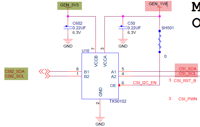
You may use I2C level shifter, this device allows having different voltage levels in the same I2C rail, below you can see an example (U10) implemented in SABRE board:
If you consider option 3 to be the best option we can provide advice and recommend and NXP I2C level shifter.
Regards,
Carlos
-----------------------------------------------------------------------------------------------------------------------
Note: If this post answers your question, please click the Correct Answer button. Thank you!
-----------------------------------------------------------------------------------------------------------------------
- 新着としてマーク
- ブックマーク
- 購読
- ミュート
- RSS フィードを購読する
- ハイライト
- 印刷
- 不適切なコンテンツを報告
Hello mert,
what device are you using?
- 新着としてマーク
- ブックマーク
- 購読
- ミュート
- RSS フィードを購読する
- ハイライト
- 印刷
- 不適切なコンテンツを報告
Hi Carlos,
I am using a physically smaller copy of imx6 quad sabre board(connections remain the same).


