- Forums
- Product Forums
- General Purpose MicrocontrollersGeneral Purpose Microcontrollers
- i.MX Forumsi.MX Forums
- QorIQ Processing PlatformsQorIQ Processing Platforms
- Identification and SecurityIdentification and Security
- Power ManagementPower Management
- Wireless ConnectivityWireless Connectivity
- RFID / NFCRFID / NFC
- MCX Microcontrollers
- S32G
- S32K
- S32V
- MPC5xxx
- Other NXP Products
- S12 / MagniV Microcontrollers
- Powertrain and Electrification Analog Drivers
- Sensors
- Vybrid Processors
- Digital Signal Controllers
- 8-bit Microcontrollers
- ColdFire/68K Microcontrollers and Processors
- PowerQUICC Processors
- OSBDM and TBDML
- S32M
-
- Solution Forums
- Software Forums
- MCUXpresso Software and ToolsMCUXpresso Software and Tools
- CodeWarriorCodeWarrior
- MQX Software SolutionsMQX Software Solutions
- Model-Based Design Toolbox (MBDT)Model-Based Design Toolbox (MBDT)
- FreeMASTER
- eIQ Machine Learning Software
- Embedded Software and Tools Clinic
- S32 SDK
- S32 Design Studio
- GUI Guider
- Zephyr Project
- Voice Technology
- Application Software Packs
- Secure Provisioning SDK (SPSDK)
- Processor Expert Software
-
- Topics
- Mobile Robotics - Drones and RoversMobile Robotics - Drones and Rovers
- NXP Training ContentNXP Training Content
- University ProgramsUniversity Programs
- Rapid IoT
- NXP Designs
- SafeAssure-Community
- OSS Security & Maintenance
- Using Our Community
-
- Cloud Lab Forums
-
- Knowledge Bases
- ARM Microcontrollers
- i.MX Processors
- Identification and Security
- Model-Based Design Toolbox (MBDT)
- QorIQ Processing Platforms
- S32 Automotive Processing Platform
- Wireless Connectivity
- CodeWarrior
- MCUXpresso Suite of Software and Tools
- MQX Software Solutions
- RFID / NFC
-
Hi,
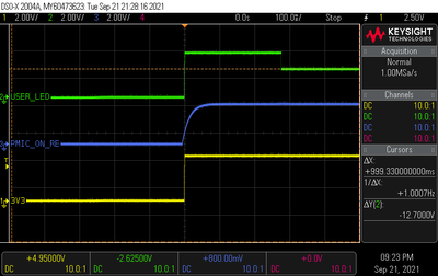
On the i.MX RT1064 EVK, using the demo blinky application (SDK v2.8.6) with MCUXpresso v11.2.1, we see that if we measure the 3v3 and PMIC_ON_REQ until the LED is actually set, it takes about ~270ms.
Using the switch to do a POR, this is almost instant.
What is taking so long to get to the application? Can this time be reduced? Are there settings in the DCD that can be tweaked?
Attached is a screenshot from our scope.
Thanks in advance,
Pieter
已解决! 转到解答。
Hi @pdgendt @kerryzhou ,
I also performed some tests with the Zephyr Blinky App loaded on the RT1064 EVK running v2.7.0-rc4. I timed from DCDC_3V3 to the LED blinking (cold boot case) was 274ms and from POR_B to LED blinking (reset case) was only 16ms, which is similar to what you got.
I did some research and found that the reason that the cold boot takes so long, is due to a voltage supervisor chip on our EVKs (labeled U2) part number UM803RS. This chip holds the POR_B signal low for a minimum of 140 ms from the time DCDC_3v3 reaches the minimum threshold voltage.
The EVK is designed to be overly conservative with this. There are power-up sequencing requirements even without the voltage supervisor. If the on-chip DCDC is used, you need at least 1ms delay from when the DCDC input voltage is stable to starting up the DCDC. And then the DCDC also has a startup time. So it's not possible to completely eliminate the power-sequencing time. The chip will have voltage monitors of it's own, to prevent the POR_B signal from being asserted internally (so you can't see it on the outside pin).
The external voltage supervisor could be removed in your custom design if desired, which would likely reduce the power-sequencing time. Just make sure to evaluate the rest of your power-sequencing needs, in case you have other power supplies that need a longer time to get up and running.
Hope this helps provide some closure and solution to the issue.
Regards,
-Manuel
Hi @pdgendt ,
Do you boot the code from the external QSPI flash, right?
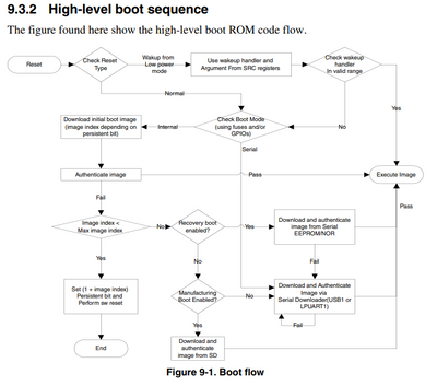
If yes, let's talk about the boot mode at first, after POR, the chip will run the internal ROM code at first, it will read the external QSPI flash FCB, then configure the flexSPI interface, then check the external memory IVT, after it is valid, it will jump to the customer code, so all these operation need the time.
I think you can set higher flexSPI frequency, eg, project xip folder, evkmimxrt1064_flexspi_nor_config.c, qspiflash_config,
Set:
.serialClkFreq = kFlexSpiSerialClk_100MHz,
to
.serialClkFreq = kFlexSpiSerialClk_133MHz,
The time may be shorten, but, about 270ms enter the user APP after POR, I think it is correct, as the ROM code, flexspi interface configuration, and jumpt to the app all need code execution time.
Wish it helps you!
Bes Regards,
Kerry
Hi @kerryzhou
We boot from the internal NOR flash (W25Q32JV), the external QSPI flash isn't used.
Can't the device configuration performance be improved, for example with the DCD data? Are there options using the boot mode/config/fuses to skip some unnecessary steps?
Still 270ms feels huge, if the customer application is able to configure the other flexspi interface in a few milliseconds.
Thanks,
Pieter
Hi @pdgendt ,
RT1064 Internal QSPI in fact is also the external QSPI, as it just put the external QSPI into the RT internal side, but the operation is the same as the external QSPI flash.
So the boot process is the same.
Do you try to modify the flexspi frequency to higher?
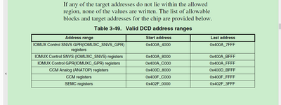
About the DCD, the supported register is:
You can find the GPIO is not in the support register.
You also can put your GPIO pull-down code in this API:SystemInit, after the watchdog disabled code, this will be executed after enter the app reset handler.
Best Regards,
Kerry
Hi @kerryzhou
The GPIO is just an example we could measure, we'd like to have the user application boot faster.
Even changing the frequency from 100 to 133 MHz would still result in a boot time, higher than 200ms right?
Hi @pdgendt ,
Do you test 133 MHz on your side? That will shorten the boot time, especially when do the code access in the QSPI flash and execution.
But the internal ROM code which is used for booting, that time can't be shorten, as it is fixed and can't be modifiy.
DCD normally used for the SEMC interface configuration for the external SDRAM initialize.
What I can suggest you is the flexSPI speed set to higher.
Best Regards,
Kerry
HI @kerryzhou
I will verify the 133 MHz and let you know what gain we got.
For the DCD you mentioned external SDRAM, can this be left out as we don't need this on our custom board. Won't this speed up the boot process as well?
Hi @pdgendt ,
Please refer to App Note 12085 on how to enable low power on the RT devices:
https://www.nxp.com.cn/docs/en/application-note/AN12085.pdf
You can also see the Power Mode Switch example available in the SDK:
RT 1064 SDK -> demo_apps -> power_mode_switch_bm or power_mode_switch_rtos
I tried to look online, but couldn't find anything on low-power wake-up times on the RT1064, so if you run any tests, please let us know the results.
It seems there's a couple different low-power modes: System Idle, Low Power Idle, Suspend, and SNVS. With each increasing in exit times. Looks like some need to disable some PLLs/Clocks, and gate some of the peripherals.
In the past, I ran a test to determine boot-times with different memories on the RT1050, and I found that they were very close to each other (all ~10ms). So I'm not sure that changing the memory clock speed or changing which memory you boot from would have much of an impact on your boot time:
I hope this helps,
-Manuel
Hi @pdgendt ,
If it is the wakeup, you will run the code directly.
But the first time you still need to run the app code which let the chip enter the low power mode.
To some low power mode, not the reset wakeup, it will run the code after the code which enters the low power directly.
Best Regards,
Kerry
Hi @pdgendt @kerryzhou ,
I also performed some tests with the Zephyr Blinky App loaded on the RT1064 EVK running v2.7.0-rc4. I timed from DCDC_3V3 to the LED blinking (cold boot case) was 274ms and from POR_B to LED blinking (reset case) was only 16ms, which is similar to what you got.
I did some research and found that the reason that the cold boot takes so long, is due to a voltage supervisor chip on our EVKs (labeled U2) part number UM803RS. This chip holds the POR_B signal low for a minimum of 140 ms from the time DCDC_3v3 reaches the minimum threshold voltage.
The EVK is designed to be overly conservative with this. There are power-up sequencing requirements even without the voltage supervisor. If the on-chip DCDC is used, you need at least 1ms delay from when the DCDC input voltage is stable to starting up the DCDC. And then the DCDC also has a startup time. So it's not possible to completely eliminate the power-sequencing time. The chip will have voltage monitors of it's own, to prevent the POR_B signal from being asserted internally (so you can't see it on the outside pin).
The external voltage supervisor could be removed in your custom design if desired, which would likely reduce the power-sequencing time. Just make sure to evaluate the rest of your power-sequencing needs, in case you have other power supplies that need a longer time to get up and running.
Hope this helps provide some closure and solution to the issue.
Regards,
-Manuel


