- Forums
- Product Forums
- General Purpose MicrocontrollersGeneral Purpose Microcontrollers
- i.MX Forumsi.MX Forums
- QorIQ Processing PlatformsQorIQ Processing Platforms
- Identification and SecurityIdentification and Security
- Power ManagementPower Management
- Wireless ConnectivityWireless Connectivity
- RFID / NFCRFID / NFC
- Advanced AnalogAdvanced Analog
- MCX Microcontrollers
- S32G
- S32K
- S32V
- MPC5xxx
- Other NXP Products
- S12 / MagniV Microcontrollers
- Powertrain and Electrification Analog Drivers
- Sensors
- Vybrid Processors
- Digital Signal Controllers
- 8-bit Microcontrollers
- ColdFire/68K Microcontrollers and Processors
- PowerQUICC Processors
- OSBDM and TBDML
- S32M
- S32Z/E
-
- Solution Forums
- Software Forums
- MCUXpresso Software and ToolsMCUXpresso Software and Tools
- CodeWarriorCodeWarrior
- MQX Software SolutionsMQX Software Solutions
- Model-Based Design Toolbox (MBDT)Model-Based Design Toolbox (MBDT)
- FreeMASTER
- eIQ Machine Learning Software
- Embedded Software and Tools Clinic
- S32 SDK
- S32 Design Studio
- GUI Guider
- Zephyr Project
- Voice Technology
- Application Software Packs
- Secure Provisioning SDK (SPSDK)
- Processor Expert Software
- Generative AI & LLMs
-
- Topics
- Mobile Robotics - Drones and RoversMobile Robotics - Drones and Rovers
- NXP Training ContentNXP Training Content
- University ProgramsUniversity Programs
- Rapid IoT
- NXP Designs
- SafeAssure-Community
- OSS Security & Maintenance
- Using Our Community
-
- Cloud Lab Forums
-
- Knowledge Bases
- ARM Microcontrollers
- i.MX Processors
- Identification and Security
- Model-Based Design Toolbox (MBDT)
- QorIQ Processing Platforms
- S32 Automotive Processing Platform
- Wireless Connectivity
- CodeWarrior
- MCUXpresso Suite of Software and Tools
- MQX Software Solutions
- RFID / NFC
- Advanced Analog
-
- NXP Tech Blogs
- Home
- :
- 製品フォーラム
- :
- Vybrid プロセッサ
- :
- Re: EXTAL stays low, crystal doesnt work
Switching Vybrid Core Power Source
- RSS フィードを購読する
- トピックを新着としてマーク
- トピックを既読としてマーク
- このトピックを現在のユーザーにフロートします
- ブックマーク
- 購読
- ミュート
- 印刷用ページ
Switching Vybrid Core Power Source
- 新着としてマーク
- ブックマーク
- 購読
- ミュート
- RSS フィードを購読する
- ハイライト
- 印刷
- 不適切なコンテンツを報告
Hello
We have some identical boards with the Vybrid Processor on it.
One of them doesnt work from the beginnings, one stopped work after some days of software testing.
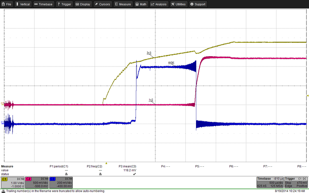
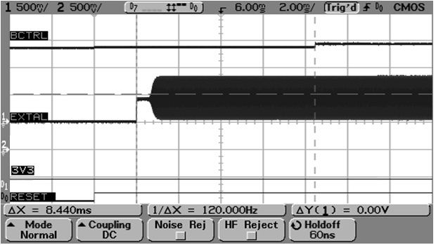
The problem is the initializing/start up of the board. When the board is powered up, the line EXTAL goes to 0.6V for about 2ms. Then its tied low again. This is identical on the good and the bad boards.
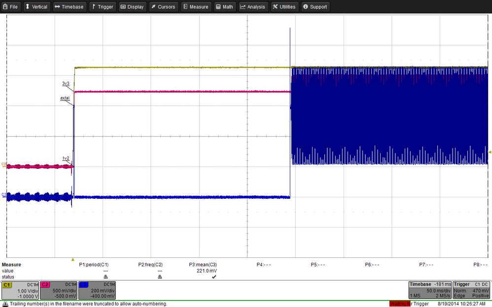
But then: the good boards set the EXTAL after a while again to 0.6V and the crystal starts working. On the bad boards EXTAL stays low, and the initialisazation stops on the Point /* Wait for PLL lock. */.
What can be the Problem? The boards are (should be) identical, the software is the same...?
Pic1 below: power up, all boards start up like this.
Pic2 below: good boards set EXTAL to 0.6V like on the pic, on bad boards EXTAL stays low forever...
Thanks in advance.
- 新着としてマーク
- ブックマーク
- 購読
- ミュート
- RSS フィードを購読する
- ハイライト
- 印刷
- 不適切なコンテンツを報告
Dear Benno,
- The first thing coming to my mind is the power-up sequence; may you send the schematic fragment showing how Vybrid is powered in your design, please?
- I would also strongly recommend to get the Vybrid Hardware Development Guide (Rev.0) - initial (unofficial) draft. document via a local Freescale FAE - you might find the answer there as well.
Sincerely, Naoum Gitnik.
- 新着としてマーク
- ブックマーク
- 購読
- ミュート
- RSS フィードを購読する
- ハイライト
- 印刷
- 不適切なコンテンツを報告
Hello Naoum
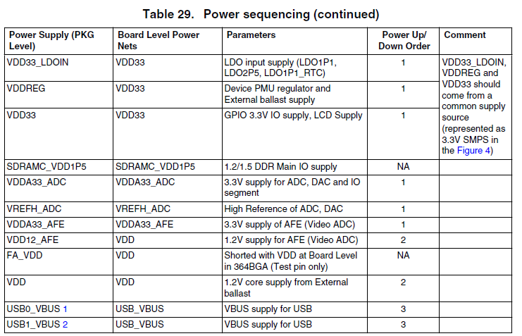
Relating to the power sequencing table from the Datasheet:
- The voltages VDD33_LDOIN, VDDREG, VDD33 are supplied from the same power rail.
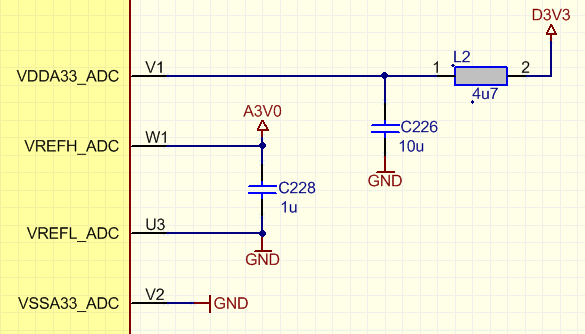
- VDD33_ADC is supplied also from the same power rail, but filtered:
- VREFH_ADC is switched on by application and comes later (but it mades no difference, when i applied this supply from beginnings)
- VDDA33_ADC is not used and tied to GND. (On the hardware development guide, its new defined to tie it to 3V3 if unused)
- The ballast transistor is anyway controlled by the controller on startup, and the other supplies are not used and tied to GND.
The controller is hold in reset state after power on for about 200ms, so all power supplies should be ok then.
The most boards are running without any problems. But one is not working, and one works sometimes. So i dont feel very comfortable for a bigger series of PCB's...
best regards
- 新着としてマーク
- ブックマーク
- 購読
- ミュート
- RSS フィードを購読する
- ハイライト
- 印刷
- 不適切なコンテンツを報告
Dear Benno,
Thanks for the information sent - everything is correct.
I would like to also see the 1.2V power rail - generation and connections.
§ (Please, also review the Vybrid Hardware Development Guide (Rev.0) - initial (unofficial) draft. document mentioned earlier. It contains a lot of fine aspects and potential design improvements.)
Sincerely, Naoum Gitnik.
- 新着としてマーク
- ブックマーク
- 購読
- ミュート
- RSS フィードを購読する
- ハイライト
- 印刷
- 不適切なコンテンツを報告
Good Morning
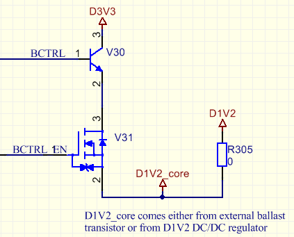
The 1V2 are generated with an external ballast transistor.
There is also the possibility to switch to another power source, but ist not used yet. (BCTRL_EN always high)
D1V2_core is connected to all VDD1-VDD23 and FA_VDD pins, and there are >20 100nF capacitors on these pins, placed as near as possible (like on the tower board).
And DECAP_V11_LDO_OUT has a 10uF capacitor.
This is the whole 1V2 power rail. I think, there can't be so much wrong?
And yes, i will have a look into the design guide....
thanks!
- 新着としてマーク
- ブックマーク
- 購読
- ミュート
- RSS フィードを購読する
- ハイライト
- 印刷
- 不適切なコンテンツを報告
[updated-2]
Dear Benno,
Thanks for the information sent.
So, the D1V2_core rail has ">20 100nF capacitors" but what about the bulk one (e.g., 4.7uF like in our designs)?
(BTW, even though "BCTRL_EN always high", I guess it comes from the processor whose code has not been finalized yet... In this case, based on my experience, it might make sense, at least for now, to "hard-wire" V31 to guarantee it it is ON (or even replaced with a short!) all the time, for sure!)
Please, also take a closer look at the Vybrid reset line - I am a bit confused by the fact that the oscillator starts at '3V3' equal to approx. 2V, then stops after a few ms when '1V2' equals approx. 0.5V (all this when the oscillator is supposed to be disabled by the reset pin's logic-low state...).
Shown below is what we observe on our boards:
As you can see, both BCTRL (i.e. 1V2, too) and 3.3V are already stable when the RESET goes high, and then the oscillator's bias goes ON, and then oscillation starts.
(The 2 upper, analog, channels are for BCTRL and 3.3V, the 2 lower, digital, channels are for 3V3 and Vybrid RESET).
Sincerely, Naoum Gitnik.
- 新着としてマーク
- ブックマーク
- 購読
- ミュート
- RSS フィードを購読する
- ハイライト
- 印刷
- 不適切なコンテンツを報告
Hello Naoum
Yes your right, it has something to do with the power up sequence.
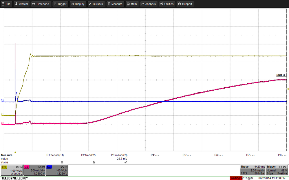
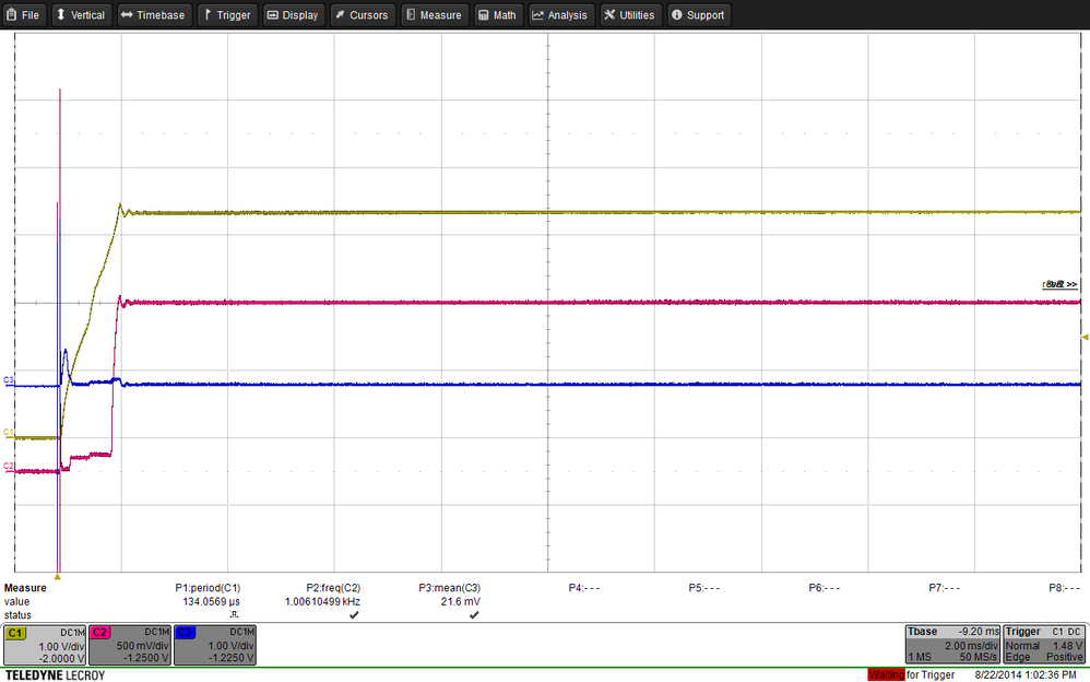
For smooth switching between ballast transistor and DC/DC supply, we switched the FET BCTRL_EN very slowly. On power up, the 1V2 supply goes up also slowly. This seems to be a problem.
On first picture below, the controller doesn't start. On second pic, it starts. (yellow: 3V3, red: 1V2). I'm bit confused, because the start sequence is the same, and the controller is the whole power up sequence in reset state anyway?
But im looking forward to solve the problem... thanks for your help!
- 新着としてマーク
- ブックマーク
- 購読
- ミュート
- RSS フィードを購読する
- ハイライト
- 印刷
- 不適切なコンテンツを報告
Dear Benno,
So, the problem is related to "switching between ballast transistor and DC/DC supply"? - It was not clear from the original data provided...
There is no need to "...switch... the FET BCTRL_EN very slowly"; it can be fast but just follow 2 rules here:
- Your D1V2, (i.e. external to Vybrid) shall be stable prior to the power source switching; based on your first scope screenshot, it looks like you do it in the opposite order - the D1V2DC/DC converter is just enabled and charges capacitors on its output.
- power coming from it and that from the ballast transistor should overlap, e.g., for a few tens of ms, until you disconnect the ballast transistor.
(All this is explained in the AN4807 "Vybrid Power Consumption and Options” Application Note.)
While testing this scheme, we simply used 2 mechanical switches and did this switching manually while watching the D1V2_core rail for any disturbances (saw none).
BTW, you provided no timing data for the RESET_B signal; I am even suspecting it is only related to 3.3V rail but not 1.2V... and, as you can see, its Logic High enables the oscillator we are discussing.
Regards, Naoum Gitnik.
- 新着としてマーク
- ブックマーク
- 購読
- ミュート
- RSS フィードを購読する
- ハイライト
- 印刷
- 不適切なコンテンツを報告
Hello Naoum
Yes it looks like the problem cames from the switching between the power rails.
We have the following problem there:
The ballast transitor is generating 1.23V, the DC/DC converter 1.2V. So when we enable the 1.2V converter, it is doing nothing because the voltage on the rail is already over 1.2V. It starts not before the voltage drops below 1.2V, so we switched slowly that the DC/DC converter had time to start working. When we first switched off the ballast transistor hard,the 1.2V falls down to 1.1V or less until the DC/DC converter could readjust the voltage.
Is this not always the problem with a DC/DC converter, they stabilize a power rail only if the voltage there drops below the target voltage? It should be possible to lower the voltage of the ballast transitor below the DC/DC converter, before it is switched off...
If we dont find a very robust circuit for switching the supplies, we will switch to the solution with a 1V5 converter, connect the ballast transistor to it and never switch it off.
The reset signal goes high 200ms after 3V3 and analog voltages are ok. Not a problem yet on startup, the 1V2 are raising with the 3V3.
Or could it be a problem in running state, when we have spikes/voltage drops on the 1V2 rail?
best regards
- 新着としてマーク
- ブックマーク
- 購読
- ミュート
- RSS フィードを購読する
- ハイライト
- 印刷
- 不適切なコンテンツを報告
[update]
Dear Benno,
The DC/DC converter's behavior you described (decreasing down to 1.1V prior to starting regulating properly) does look right to me. How can that be if its output capacitior is fully charged prior to connecting on the 1V2 rail bearing 1.23V?
I am providing the schematic of what we tested; quite likely it has a different DC/DC converter, but it is still unclear what is causing a significant voltage dip in your case.
(Ignore the 1.8V option in the attached file, focus on the 1.2V one only.)
By the way, why are you using the external 1.2V option? You do not have DDR, right? If so, Vybrid does not run heavy computations hence consumes significantly less power (than when DDR is used) and dissipates much less heat on the ballast transistor even with 3.3V on its collector. If in this case you are having a DC-DC converter only for Vybrid, it makes your design noticeably more expensive.
Regards, Naoum Gitnik.
- 新着としてマーク
- ブックマーク
- 購読
- ミュート
- RSS フィードを購読する
- ハイライト
- 印刷
- 不適切なコンテンツを報告
Hi Naoum
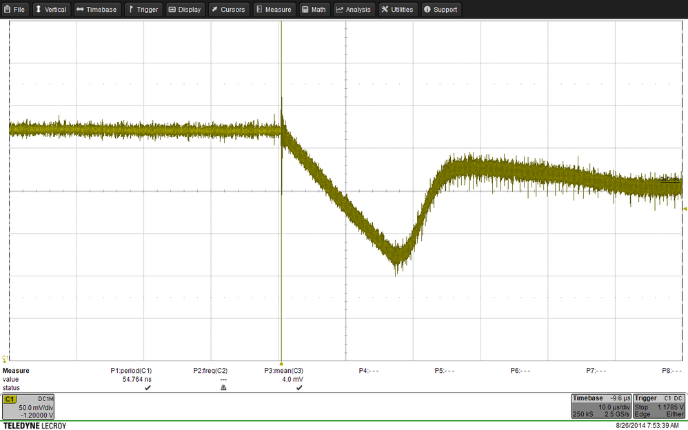
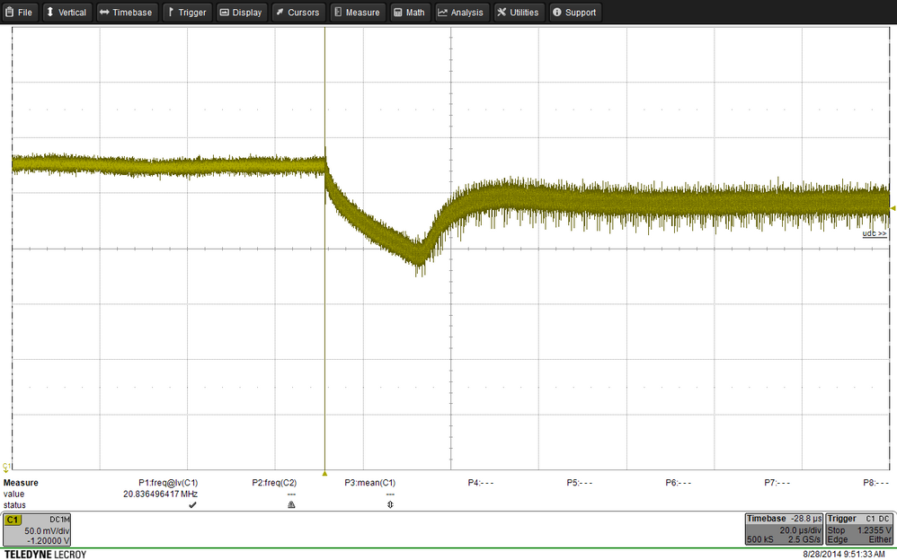
Heres a picture from the power switching. The ballast transistor (~1.26V) is hard switched off. The DC/DC converter starts working when the voltage drops below 1.2V, and then it needs about 12us to stabilize the voltage.(10us/div, 50mV/div). This is enough for the voltage to fall to 1.12V. I think, this is the case with every DC/DC converter, when the voltage of the ballast transistor is over the output of the converter? Or what looks like the VDD switching on your boards?
This was the reason to switch the ballast transistor slowly, then we could minimize the voltage drop to 20mV or so.
We dont use DDR. But we have a current of about 300mA on the 1.2V when we made some tests with a lot of hard calculations. This is a power loss of about 0.6W only on the ballast transistor. This is too much for our application.
So i think, for the moment we go with an 1.5V converter and an always enabled ballast transitor.
Regards Benno
- 新着としてマーク
- ブックマーク
- 購読
- ミュート
- RSS フィードを購読する
- ハイライト
- 印刷
- 不適切なコンテンツを報告
Dear Benno,
Thanks - it is clear now why you are saving power.
Please, confirm that you FULLY follow the below procedure:
- let Vybrid start up the regular way (using the linear core regulator),
- enable external DC-DC converter,
- wait (units to tens of ms) until voltage on the DC-DC converter's output capacitor stabilizes,
- when external 1.2V is stable, connect the DC-DC converter's output capacitor to the Vybrid core rail,
- wait (units to tens of ms) keeping the 2 core power sources overlapped,
- disconnect the linear core regulator (ballast transistor's emitter) from the Vybrid core,
- :smileyhappy: enjoy running the core from the efficient DC-DC converter :smileyhappy:
Regarding what we observed with the solution I sent you earlier: we only have verbal data from the test engineer that there were no disruptions on the Vybrid core power rail.
Regards, Naoum Gitnik.
- 新着としてマーク
- ブックマーク
- 購読
- ミュート
- RSS フィードを購読する
- ハイライト
- 印刷
- 不適切なコンテンツを報告
Hello Naoum
We follow this procedure, with the difference, that we have connected the converter directly the 1V2 with no additional switch. (A switch in the power rail would have also power losses we dont want) So the capacitors from the converter are already preloaded to 1.23V when we enable the converter. This means, the current through the inductor of the converter is zero after enabling, and when we switch off the ballast transistor the current there has to increase from zero to the required value.
But its the same with an additional switch (i tried it). When the converter is disconnected, it loads his capacitors to 1.2V, and then the current through the inductor is also zero. and later on the switching, we have the same problem.
I wonder how others solve the switching between the power sources? Using smaller inductors, faster converters, bigger capacitors? but the main problem stays the same...
Regards, Benno
- 新着としてマーク
- ブックマーク
- 購読
- ミュート
- RSS フィードを購読する
- ハイライト
- 印刷
- 不適切なコンテンツを報告
Dear Benno,
- While developing our procedure, we tried to disturb normal operation of both linear and switch-mode voltage regulators as little as possible. This is why they only work "abnormally" while having their outputs temporarily connected to each other (i.e. while "overlapping" on the Vybrid core power rail). You are following this principle for the linear regulator but forcing the switch-mode one into the operating mode it is not designed for - with its output capacitor fully charged prior to turning it ON. Thus, your questions about its behavior are rather to those who designed the switch-mode voltage regulator you are using, not us.
- You asked about the capacitance values; based on the schematic I sent, you can see that the switch-mode voltage regulator's output capacitor (150uF) is significantly larger than that used on the linear one's output (5 to 10uF); thus, when they get connected in parallel, the larger one dominates, which results in very low voltage change on the switch-mode voltage regulator's output.
- Unfortunately, I do not know details of how the other several customers, which used this approach, designed this section. I only know that they asked for our schematic (the one I sent you), had some timing issues while switching rails but resolved them later with our guidance. Based on their questions, my impression was that they fully followed our scheme.
- I am a bit confused by your "... it's the same with an additional switch (I tried it)..." phrase; do you mean you actually tested 100% our scheme (with 2 switches and our timing) and still observed serious voltage dip?
Sincerely, Naoum Gitnik.
- 新着としてマーク
- ブックマーク
- 購読
- ミュート
- RSS フィードを購読する
- ハイライト
- 印刷
- 不適切なコンテンツを報告
Hello Naoum
Yes a voltage dip is always there, as long as the voltage from the converter is lower as the voltage from the ballast transistor.
With the resistors on the converter feedback loop, the converters output is some a little higher than 1.2V (1.23V or so). This means, the voltage dip is not as deep as before.
And with a higher capacitance on the rail 150uF, the voltage falls slower after powering off the ballast transistor. So the converter has some more time to start work.
With this modifications, the voltage dip is not lower than 1.2 or 1.19V. This should be ok, if it is the same under all conditions.
On datasheet, i found only a minimum required capacitance on power rail (4.7uF) and no maximum. So it should also be ok to have there 150uF directly connected to the 1.2V rail. The power rail need some time more to reach the voltage, thats all.
For a smooth power source switching, a possibility would be good to lower the reference voltage of the ballast transistor below the voltage of dcdc converter. Than the converter would have time to take control over the power rail while the voltage is still stabilized.
Best regards, Benno
- 新着としてマーク
- ブックマーク
- 購読
- ミュート
- RSS フィードを購読する
- ハイライト
- 印刷
- 不適切なコンテンツを報告
Dear Benno,
- On all our boards we have only used up to 10uF bulk capacitors on the Vybrid core rail. Although formally there is no max. value provided for it in the Datasheet, I would not use as high value as 150uF connected to the transistor emitter during the Vybrid's linear regulator's power-up - the charge time becomes much longer and, as far as I know, such a scenario has not been tested.
- Just to make it clear - this capacitance value in the Datasheet is NOT for the linear/switch-mode “combo” topology but for the linear one only (since not everybody uses this “combo” approach). This is why our approach is to let the linear and the switch-mode regulators power up first independently from each other, stabilize their output voltages, and only then connect the charged switch-mode regulator’s output capacitor in parallel to that of the linear one.
- So, it is good that, with 150uF, the voltage dip is no longer causing operation failures; however, the approach you are using differs from ours, has not been tested, and, I am afraid, you will have to use it on your own risk.
- Unfortunately, there is no way to change the linear voltage regulator's output voltage - it is fixed on the production stage.
Regards, Naoum Gitnik.
- 新着としてマーク
- ブックマーク
- 購読
- ミュート
- RSS フィードを購読する
- ハイライト
- 印刷
- 不適切なコンテンツを報告
Hello Naoum
On power up, ballast transistor will be activated and external capacitors on 1.2V rail are charged by ballast transistor i think? Then this should be ok. (No overload of internal linear regulator)
The only point is, that i have a voltage overswing of 0.4V on the 1.2V rail at power up. But i cant find any absolute maximum ratings for the 1.2V?
For the solution with switches:
If we use a switch in the 1.2V rail as you recommend, then we have unwanted power losses in the 1.2V power rail, and still a power source switching procedure.
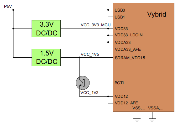
Then we could also use an 1.5V converter with an always enabled ballast transistor instead, and have no more power switching issues? (Picture below from application note). The power losses from a switch and from the ballast transistor are more or less the same in this case.
So, in the application note, the collector is connected to 1.5V.
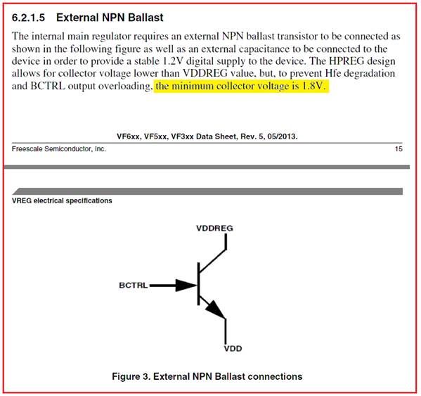
But in the datasheet, the collector voltage is specified for at least 1.8V? Or does i understand something wrong?
regards
Benno
- 新着としてマーク
- ブックマーク
- 購読
- ミュート
- RSS フィードを購読する
- ハイライト
- 印刷
- 不適切なコンテンツを報告
Dear Benno,
- Regarding 1.2V rail characteristics... This rail is internally regulated, so there is no really max. value in the meaning you are seeking; at the same time, most likely you may use the max. value from the Datasheet table called "HPREG electrical characteristics".
- If you power the ballast transistor's collector from 1.5V (or even lower - see details below), i.e. the transistor always stays "in the game", there is no switching issues.
- Regarding the ballast transistor's collector voltage lower than 1.8V mentioned in the Datasheet (you may skip directly to item 3 below):
- Using 1.8V is based ONLY on the requirements for the transistor defined in the Datasheet itself. At the same time, in the "example cases" clause on page 17, it reads "By selecting an appropriate high-beta, low-VBE transistor, a lower collector voltage is possible." - meaning lower than 1.8V.
- Details of the above approach have been discuss on the Community several times; the thread most relevant for your case is Re: Power supply for Vybrid core.
- We are currently working on the document containing all these details (all in one place!); please, see the relevant draft chapter thereof attached. The entire document (quite recommended to prevent all the possible design issues) is available via your local Freescale support person.
Regards, Naoum Gitnik.
