- Forums
- Product Forums
- General Purpose MicrocontrollersGeneral Purpose Microcontrollers
- i.MX Forumsi.MX Forums
- QorIQ Processing PlatformsQorIQ Processing Platforms
- Identification and SecurityIdentification and Security
- Power ManagementPower Management
- Wireless ConnectivityWireless Connectivity
- RFID / NFCRFID / NFC
- Advanced AnalogAdvanced Analog
- MCX Microcontrollers
- S32G
- S32K
- S32V
- MPC5xxx
- Other NXP Products
- S12 / MagniV Microcontrollers
- Powertrain and Electrification Analog Drivers
- Sensors
- Vybrid Processors
- Digital Signal Controllers
- 8-bit Microcontrollers
- ColdFire/68K Microcontrollers and Processors
- PowerQUICC Processors
- OSBDM and TBDML
- S32M
- S32Z/E
-
- Solution Forums
- Software Forums
- MCUXpresso Software and ToolsMCUXpresso Software and Tools
- CodeWarriorCodeWarrior
- MQX Software SolutionsMQX Software Solutions
- Model-Based Design Toolbox (MBDT)Model-Based Design Toolbox (MBDT)
- FreeMASTER
- eIQ Machine Learning Software
- Embedded Software and Tools Clinic
- S32 SDK
- S32 Design Studio
- GUI Guider
- Zephyr Project
- Voice Technology
- Application Software Packs
- Secure Provisioning SDK (SPSDK)
- Processor Expert Software
- Generative AI & LLMs
-
- Topics
- Mobile Robotics - Drones and RoversMobile Robotics - Drones and Rovers
- NXP Training ContentNXP Training Content
- University ProgramsUniversity Programs
- Rapid IoT
- NXP Designs
- SafeAssure-Community
- OSS Security & Maintenance
- Using Our Community
-
- Cloud Lab Forums
-
- Knowledge Bases
- ARM Microcontrollers
- i.MX Processors
- Identification and Security
- Model-Based Design Toolbox (MBDT)
- QorIQ Processing Platforms
- S32 Automotive Processing Platform
- Wireless Connectivity
- CodeWarrior
- MCUXpresso Suite of Software and Tools
- MQX Software Solutions
- RFID / NFC
- Advanced Analog
-
- NXP Tech Blogs
- Home
- :
- Product Forums
- :
- Sensors
- :
- Re: MM9Z1_638 Microcontroller GPIOB Input Set Problem
MM9Z1_638 Microcontroller GPIOB Input Set Problem
- Subscribe to RSS Feed
- Mark Topic as New
- Mark Topic as Read
- Float this Topic for Current User
- Bookmark
- Subscribe
- Mute
- Printer Friendly Page
MM9Z1_638 Microcontroller GPIOB Input Set Problem
- Mark as New
- Bookmark
- Subscribe
- Mute
- Subscribe to RSS Feed
- Permalink
- Report Inappropriate Content
Hello All,
I'am programming MM9Z1_638 microcontroller. I set output and input PORTA, but i don't set input GPIOB.
I wrote this function:
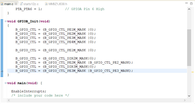
void GPIOB_Init(void)
{
B_GPIO_CTL = (B_GPIO_CTL_PE1M_MASK |0);
B_GPIO_CTL = (B_GPIO_CTL_PE2M_MASK |0);
B_GPIO_CTL = (B_GPIO_CTL_PE3M_MASK |0);
B_GPIO_CTL = (B_GPIO_CTL_PE4M_MASK |0);
B_GPIO_CTL = (B_GPIO_CTL_PE1M_MASK |0);
B_GPIO_CTL = (B_GPIO_CTL_DIR2M_MASK|0);
B_GPIO_CTL = (B_GPIO_CTL_PE2M_MASK |B_GPIO_CTL_PE2_MASK);
B_GPIO_CTL = (B_GPIO_CTL_DIR3M_MASK|0);
B_GPIO_CTL = (B_GPIO_CTL_PE3M_MASK |B_GPIO_CTL_PE3_MASK);
}
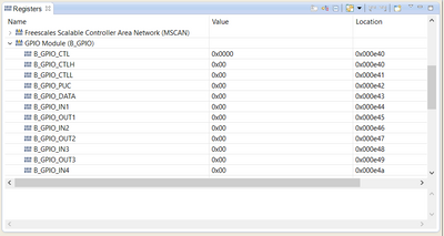
and i wath B_GPIO register and B_GPIO_CTL register is 0x0000.
Why cant i set port and how can i use this port?
- Mark as New
- Bookmark
- Subscribe
- Mute
- Subscribe to RSS Feed
- Permalink
- Report Inappropriate Content
Hello Muhammed,
No problem, just note the B_GPIO_CTL register has different bit’s meaning from the commonly used standards.
The *_MASK bits block (“0”) or allow (“1”) to write value into data bit. So if you want to have all port’s bits accessible you need use:
void GPIOB_Init(void)
{
B_GPIO_CTLH = (B_GPIO_CTLH_PE1M_MASK | // enable write to PE1;
B_GPIO_CTLH_PE2M_MASK | // enable write to PE2;
B_GPIO_CTLH_PE3M_MASK | // enable write to PE3;
B_GPIO_CTLH_PE4M_MASK | // enable write to PE4;
B_GPIO_CTLH_DIR1M_MASK | // enable write to DIR1;
B_GPIO_CTLH_DIR2M_MASK | // enable write to DIR2;
B_GPIO_CTLH_DIR3M_MASK); // enable write to DIR3;
// and then write values to low byte of B_GPIO_CTLL register;
B_GPIO_CTLL = (B_GPIO_CTLL_PE1_MASK | // PE1 enabled;
B_GPIO_CTLL_PE2_MASK | // PE2 enabled;
B_GPIO_CTLL_PE3_MASK | // PE3 enabled;
B_GPIO_CTLH_DIR1_MASK | // PE1 as output;
B_GPIO_CTLH_DIR2_MASK | // PE2 as output;
B_GPIO_CTLH_DIR3_MASK ); // PE3 as output;
}
Sorry I don’t have the board with MCU for test, but I hope my suggestion could help you.
Best Regards,
Stano.
- Mark as New
- Bookmark
- Subscribe
- Mute
- Subscribe to RSS Feed
- Permalink
- Report Inappropriate Content
Hello StanoA,
I tried the way you said but it is not work.
My init function:
Not: I want to use input GPIOB pins.
void GPIOB_Init(void)
{
B_GPIO_CTLH = (B_GPIO_CTLH_PE1M_MASK | B_GPIO_CTLH_PE2M_MASK | B_GPIO_CTLH_PE3M_MASK | B_GPIO_CTLH_PE4M_MASK
| B_GPIO_CTLH_DIR1M_MASK | B_GPIO_CTLH_DIR2M_MASK | B_GPIO_CTLH_DIR2M_MASK);
B_GPIO_CTLL = (B_GPIO_CTLL_PE1_MASK | B_GPIO_CTLL_PE2_MASK | B_GPIO_CTLL_PE3_MASK | B_GPIO_CTLL_PE4_MASK);
}
After the work, B_GPIO_C register value is 0x0000.
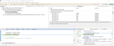
My init function:
- Mark as New
- Bookmark
- Subscribe
- Mute
- Subscribe to RSS Feed
- Permalink
- Report Inappropriate Content
Hello Muhammed,
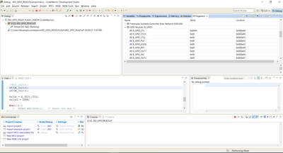
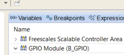
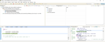
Please reset the MCU in debug mode, set the breakpoint to line “for(;;) { …” and run the code. When it will stop on breakpoint read the variables:
value and value2.
This means select them in window:
And check the values.
Best Regards,
Stano.
- Mark as New
- Bookmark
- Subscribe
- Mute
- Subscribe to RSS Feed
- Permalink
- Report Inappropriate Content
Hello StanoA,
I reset mcu in debug mode and set break point in for loop, i see the all values is 0.
- Mark as New
- Bookmark
- Subscribe
- Mute
- Subscribe to RSS Feed
- Permalink
- Report Inappropriate Content
Hello Muhammed,
I asked our specialist for help. The result is:
The port bit must be written together with their mask bit = 1.
If the associated mask bit = 0, the write is not allowed.
The masked bits (e.g. GPIO...PE1M and GPIO...PE1) have to be written in a single access. In this case as 16bit write. Please see the attached gpio.h file also for this example:
//-------------------------------------------------
// enable PTB1 as output
B_GPIO_CTL = GPIO_CTL_PTB1_ENABLE | GPIO_CTL_PTB1_OUTPUT;
B_GPIO_OUT1 = OUT_PTBx;
// set PTB1
B_GPIO_OUT1 = OUT_PTBx;
// clear PTB1
B_GPIO_OUT1 = 0;
//----------------------------------------------------
Please see also this AN for this product:
https://www.nxp.com/docs/en/application-note/AN12301.pdf
I hope it could help you with your task.
Best Regards,
Stano.
