- Forums
- Product Forums
- General Purpose MicrocontrollersGeneral Purpose Microcontrollers
- i.MX Forumsi.MX Forums
- QorIQ Processing PlatformsQorIQ Processing Platforms
- Identification and SecurityIdentification and Security
- Power ManagementPower Management
- Wireless ConnectivityWireless Connectivity
- RFID / NFCRFID / NFC
- Advanced AnalogAdvanced Analog
- MCX Microcontrollers
- S32G
- S32K
- S32V
- MPC5xxx
- Other NXP Products
- S12 / MagniV Microcontrollers
- Powertrain and Electrification Analog Drivers
- Sensors
- Vybrid Processors
- Digital Signal Controllers
- 8-bit Microcontrollers
- ColdFire/68K Microcontrollers and Processors
- PowerQUICC Processors
- OSBDM and TBDML
- S32M
- S32Z/E
-
- Solution Forums
- Software Forums
- MCUXpresso Software and ToolsMCUXpresso Software and Tools
- CodeWarriorCodeWarrior
- MQX Software SolutionsMQX Software Solutions
- Model-Based Design Toolbox (MBDT)Model-Based Design Toolbox (MBDT)
- FreeMASTER
- eIQ Machine Learning Software
- Embedded Software and Tools Clinic
- S32 SDK
- S32 Design Studio
- GUI Guider
- Zephyr Project
- Voice Technology
- Application Software Packs
- Secure Provisioning SDK (SPSDK)
- Processor Expert Software
- Generative AI & LLMs
-
- Topics
- Mobile Robotics - Drones and RoversMobile Robotics - Drones and Rovers
- NXP Training ContentNXP Training Content
- University ProgramsUniversity Programs
- Rapid IoT
- NXP Designs
- SafeAssure-Community
- OSS Security & Maintenance
- Using Our Community
-
- Cloud Lab Forums
-
- Knowledge Bases
- ARM Microcontrollers
- i.MX Processors
- Identification and Security
- Model-Based Design Toolbox (MBDT)
- QorIQ Processing Platforms
- S32 Automotive Processing Platform
- Wireless Connectivity
- CodeWarrior
- MCUXpresso Suite of Software and Tools
- MQX Software Solutions
- RFID / NFC
- Advanced Analog
-
- NXP Tech Blogs
- Home
- :
- Product Forums
- :
- S32K
- :
- S32K146 conversion frequency
S32K146 conversion frequency
- Subscribe to RSS Feed
- Mark Topic as New
- Mark Topic as Read
- Float this Topic for Current User
- Bookmark
- Subscribe
- Mute
- Printer Friendly Page
- Mark as New
- Bookmark
- Subscribe
- Mute
- Subscribe to RSS Feed
- Permalink
- Report Inappropriate Content
Hello!
IN my application,I needs collect 24 channels of ADC channel. ADC0 14 channels,ADC1 10 channels.I use back to back modes.I use DMA store ADC data.
At present, I have realized the correct collection and transmission of data. I want improve the conversion rate.In my APP,After the ADC0 channel has completed acquisition, in the DMA interrupt, turn on PDB1 to trigger ADC1 conversion.
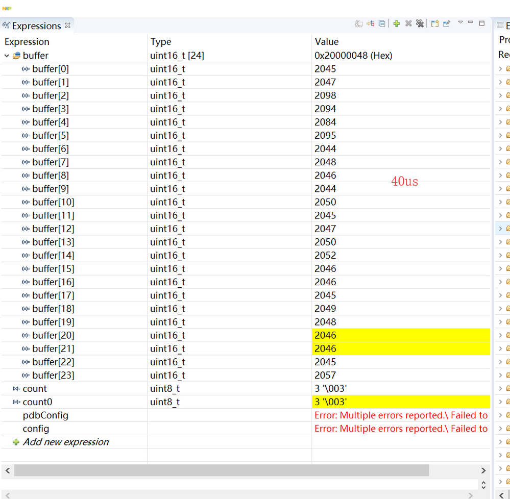
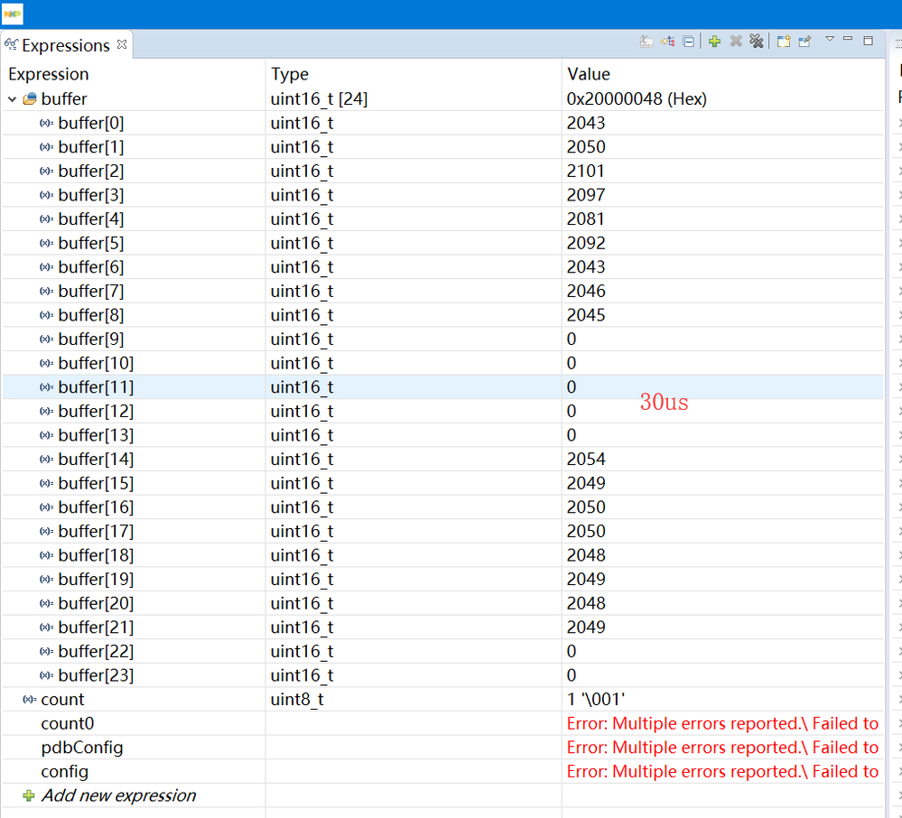
I tried to change the trigger time of the PDB. When it is changed to less than 40us, the collected data is incorrect. Will not enter the DMA interrupt.

The ADC clock is 48MHz. Sys_CLK is 112MHz.
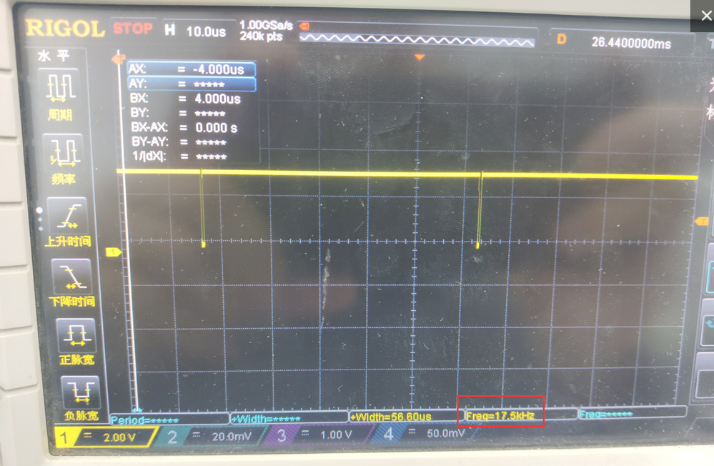
so how i can improve conversion frequency? IHow to increase the sampling rate to 25Khz?
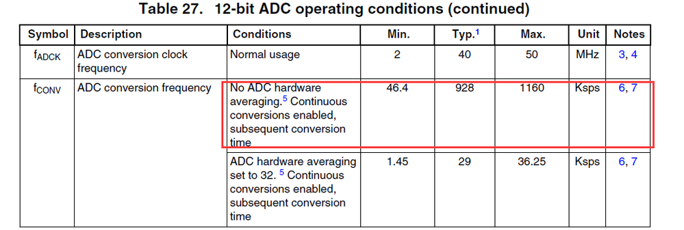
In s32kxxx datasheet,
so i try continues modes:
1、Software triggered, single channel, continuous mode for transfer suppression.
2、Software trigger, multi-channel ADC channel, when using continuous mode, only the first channel has data, and other channels have no data.
3、PDB hardware trigger, multi-channel ADC channel, does not work when using continuous mode.
Solved! Go to Solution.
- Mark as New
- Bookmark
- Subscribe
- Mute
- Subscribe to RSS Feed
- Permalink
- Report Inappropriate Content
Hi,
1. ADC sample time should be calculated to keep min value defined in the DS, which is 275ns. So with 48MHZ ADC clock it is 275ns*48MHz = 13.2. So set (14-1) into ADC inspector's sample time parameter.
2. the PBD timer should be properly set. Did you check what value is calculated for "delayValue"? It was 3, so you completely lost a precision for placing delay for PDB channel 1. So choose prescaler divider = 1 in both PDBs setting. This gives you better result for delayValue. Finaly set proper value for PDB channel 1 delay0 register, based on real ADC conversion time. I used below instructions to set a delay for 9us...
PDB_DRV_SetAdcPreTriggerDelayValue(INST_PDLY0, 1UL, 0UL,(uint32_t) (9*delayValue/PDLY_TIMEOUT));
PDB_DRV_SetAdcPreTriggerDelayValue(INST_PDLY1, 1UL , 0UL , (uint32_t) (9*delayValue/PDLY_TIMEOUT));
3. Start PDB0 after PDB1 is completely set.
See attached hw_init.c I modified to make the example running. For the sequential conversion you are using the DMA1 interrupt is called approx each 30us.
For sure you can start both PDBs at the same time, so conversions can run parallel. Start both PDBs in the DMA0 interrupt which is called later, ADC0 sequence is longer. This way you can get even shorter time for DMA0 interrupt, about 18us. See api_dma.c.
BR, Petr


