
- Forums
- Product Forums
- General Purpose MicrocontrollersGeneral Purpose Microcontrollers
- i.MX Forumsi.MX Forums
- QorIQ Processing PlatformsQorIQ Processing Platforms
- Identification and SecurityIdentification and Security
- Power ManagementPower Management
- Wireless ConnectivityWireless Connectivity
- RFID / NFCRFID / NFC
- Advanced AnalogAdvanced Analog
- Neural Processing UnitsNeural Processing Units
- MCX Microcontrollers
- S32G
- S32K
- S32V
- MPC5xxx
- Other NXP Products
- S12 / MagniV Microcontrollers
- Powertrain and Electrification Analog Drivers
- Sensors
- Vybrid Processors
- Digital Signal Controllers
- 8-bit Microcontrollers
- ColdFire/68K Microcontrollers and Processors
- PowerQUICC Processors
- OSBDM and TBDML
- S32M
- S32Z/E
-
- Solution Forums
- Software Forums
- MCUXpresso Software and ToolsMCUXpresso Software and Tools
- CodeWarriorCodeWarrior
- MQX Software SolutionsMQX Software Solutions
- Model-Based Design Toolbox (MBDT)Model-Based Design Toolbox (MBDT)
- FreeMASTER
- eIQ Machine Learning Software
- Embedded Software and Tools Clinic
- S32 SDK
- S32 Design Studio
- GUI Guider
- Zephyr Project
- Voice Technology
- Application Software Packs
- Secure Provisioning SDK (SPSDK)
- Processor Expert Software
- Generative AI & LLMs
-
- Topics
- Mobile Robotics - Drones and RoversMobile Robotics - Drones and Rovers
- NXP Training ContentNXP Training Content
- University ProgramsUniversity Programs
- Rapid IoT
- NXP Designs
- SafeAssure-Community
- OSS Security & Maintenance
- Using Our Community
-
- Cloud Lab Forums
-
- Knowledge Bases
- ARM Microcontrollers
- i.MX Processors
- Identification and Security
- Model-Based Design Toolbox (MBDT)
- QorIQ Processing Platforms
- S32 Automotive Processing Platform
- Wireless Connectivity
- CodeWarrior
- MCUXpresso Suite of Software and Tools
- MQX Software Solutions
- RFID / NFC
- Advanced Analog
- Neural Processing Units
-
- NXP Tech Blogs
- Home
- :
- Product Forums
- :
- S32K
- :
- Re: MDIORead always returning 0xFFFF on RMII interface
MDIORead always returning 0xFFFF on RMII interface
- Subscribe to RSS Feed
- Mark Topic as New
- Mark Topic as Read
- Float this Topic for Current User
- Bookmark
- Subscribe
- Mute
- Printer Friendly Page
MDIORead always returning 0xFFFF on RMII interface
- Mark as New
- Bookmark
- Subscribe
- Mute
- Subscribe to RSS Feed
- Permalink
- Report Inappropriate Content
Hi, I've been working with a s32k148 and a Microchip LAN8720A phy daughterboard trying to get them to communicate. I designed a mating PCB to route the signals from the phy to the J16 connector. I've been able to get the phy properly initialized at power on and Im able to see an amber and green LED when I plug it into my Windows computer as well as wireshark activity from the PC side. The next step is to have the MAC interface of the board talk with the phy but thats where the issue arrises. I've setup my code to copy the tja1101 exemple as closely as possible but everytime I try to run it the ENET_DRV_MDIORead() inside PHY_SHARED_ReadBasicStatus() in the mainfunction instruction returns 0xFFFF.
heres a list of the things I've double checked :
- 50MHz clock is withing specs and is on both the CLKIN pin of the phy and PTD11 of J16.
- The MDC frequency given by the internal module clock and the MII_SPEED bit is 2.4MHz (Internal module clock = 48MHz and MII_SPEED bit = 9).
- The phy address is 0 per the datasheet (RXER/PHYADD0 pulled low internally)
I've attached my entire project to this post so I can make sure that my initialization code is fine as well as datasheet for the phy.
I've also measured activity on the MDIO and MDC line using my oscilloscope but I cannot tell wether it was proper form or not.
Thanks!
- Mark as New
- Bookmark
- Subscribe
- Mute
- Subscribe to RSS Feed
- Permalink
- Report Inappropriate Content
Have you tried scanning other PHY addresses just in case? I’ve seen cases where the strapping didn’t take effect properly and the PHY came up on a different address than expected.
- Mark as New
- Bookmark
- Subscribe
- Mute
- Subscribe to RSS Feed
- Permalink
- Report Inappropriate Content
- Mark as New
- Bookmark
- Subscribe
- Mute
- Subscribe to RSS Feed
- Permalink
- Report Inappropriate Content
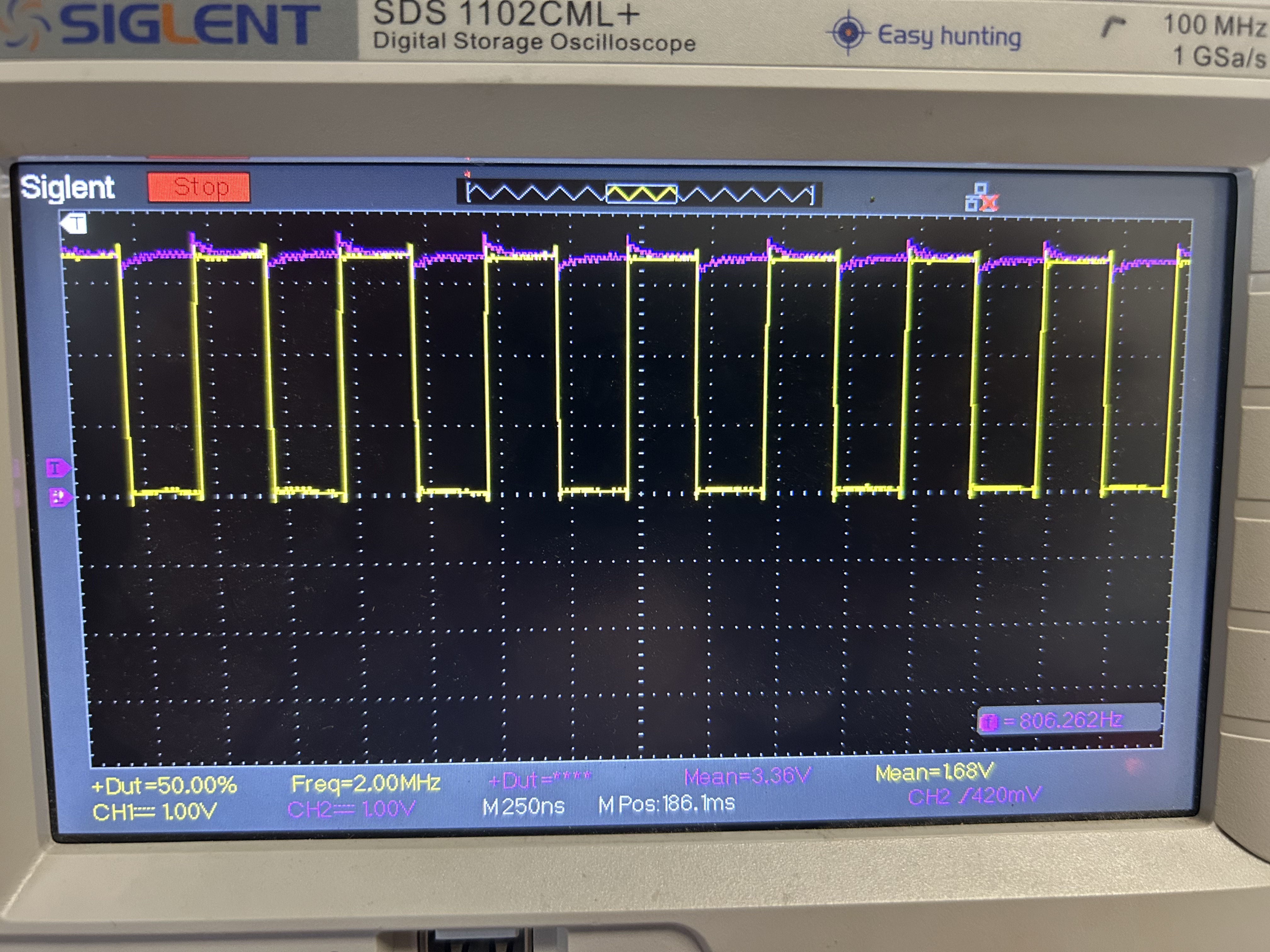
Update on the situation, I found out the I did not mux the right pin for MDC, and after changing it the MDC signal is perfect at 2MHz. However, I still have issues with MDIO stability. The Mac is able to read from the phy but the link stability is awful. Ive attached some picture of MDIO reading from my oscilloscope. Ive come to understand that pin PTB4 which is MII_RMII_MDIO should be an open-drain in order to let both the MAC and the phy write to it. However I dont see that option inside the pin muxing menu and its locked as an input/output pin. I get the impression that the phy and the mac are fighting for it for some reason. also the signal around the 3.3V on the pictures looks like discharge/charge curves.
- Mark as New
- Bookmark
- Subscribe
- Mute
- Subscribe to RSS Feed
- Permalink
- Report Inappropriate Content
- Mark as New
- Bookmark
- Subscribe
- Mute
- Subscribe to RSS Feed
- Permalink
- Report Inappropriate Content
- Mark as New
- Bookmark
- Subscribe
- Mute
- Subscribe to RSS Feed
- Permalink
- Report Inappropriate Content
Hello @christopherlajoie ,
I have reviewed all available configuration files, initialization code, and oscilloscope captures provided. The MDC signal is now correctly configured and operating at 2.4 MHz. The MDIO line has a proper 1.5 kΩ external pull-up resistor, and the ENET peripheral is correctly initialized. Based on this, the remaining issue appears to be related to signal observation rather than functional failure.
Thank you for the update and sharing all your data. Based on your description and the oscilloscope captures, the MDIO signal instability you’re observing is most likely due to undersampling.
- Each MDIO transaction (Clause-22 read) consists of 64 bits, clocked at ~2.4 MHz → total duration ~27 µs.
- With a time base of 500 µs/div, the oscilloscope may only capture a few samples per transaction.
- This can result in distorted or partial waveforms that resemble discharge/charge curves or “V-shape” dips.
Since the PHY read is now returning valid data, and the MDC signal is confirmed to be correct, the MDIO line is likely functioning properly.
Recommended next step:
- Set the oscilloscope to 1–5 µs/div.
- Trigger on MDC rising edge.
- Capture in single-shot mode during a known PHY_Read().
This will allow you to observe the full MDIO transaction and confirm signal integrity.
Best regards,
Pavel
- Mark as New
- Bookmark
- Subscribe
- Mute
- Subscribe to RSS Feed
- Permalink
- Report Inappropriate Content
Hi PaveIL,
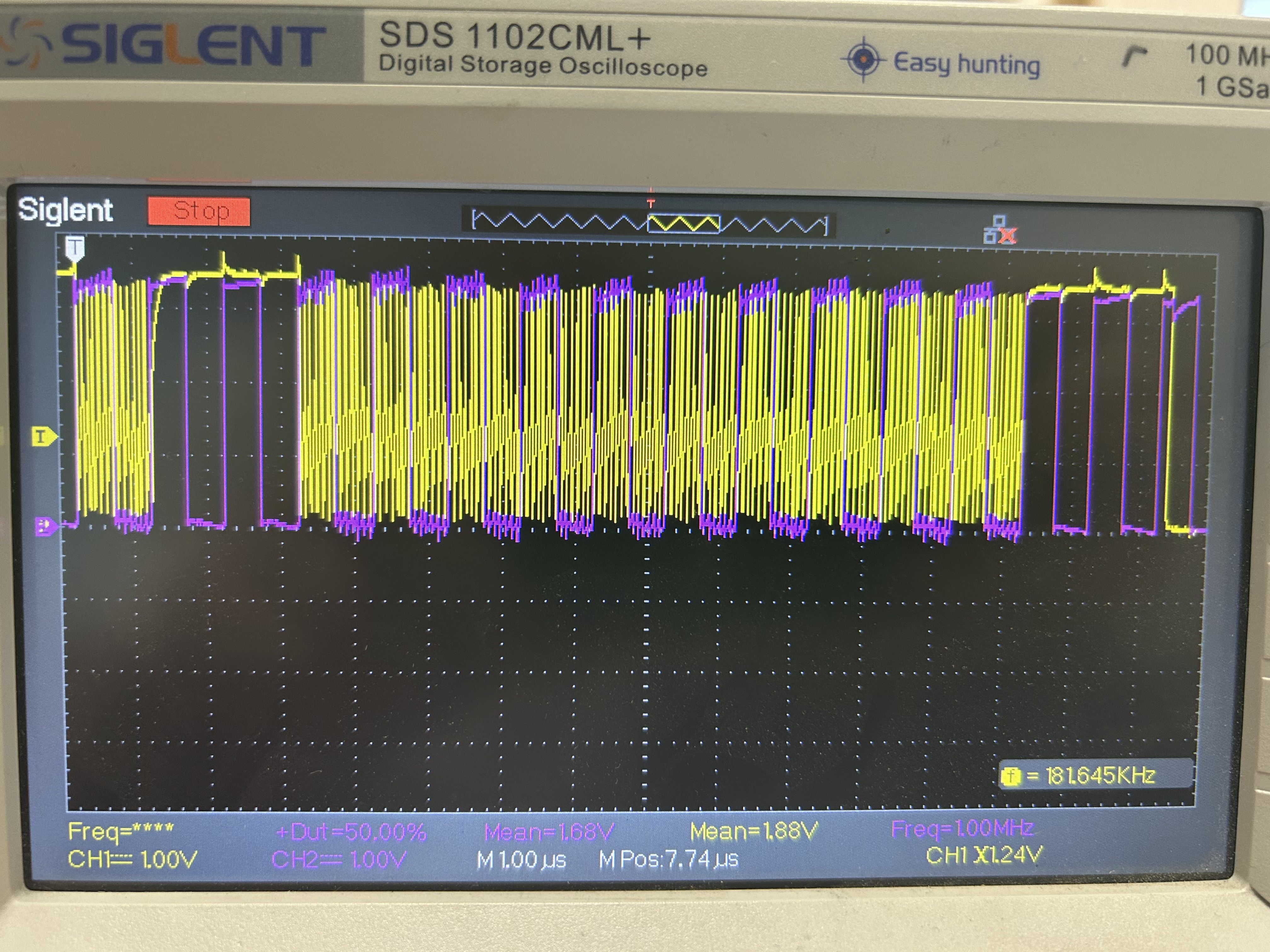
Thanks a lot for your input, you are right about the undersampling I was indeed not reading the signal correctly. I've sampled it properly and here are my findings:
- On every PHY_read() transaction it seems the MAC writing on the MDIO bus part of the signal is all over the place, but the PHY writing on the bus looks clean.
- From the pictures I linked it seems that the MAC isnt properly able to pull the line low to send logic 0's and that results in very sharp spikes between 0V and 3.3V during the entire write duration.
- The timing of the writes seem fine from what I could see.
I looked into it and Im wondering if its not an issue with the MDIO/PTB4 pin of the J16 connector. I've got it configured properly as you can see below but it doesnt seem to behave as an open-drain collector. Am I missing some configuration?
Ive modified the config to set MDC frequency to 1 MHz which is why its reading 1 MHz on the pictures. Also the hold time is set to 3 module clock cycles at 48MHz.

Thanks!
- Mark as New
- Bookmark
- Subscribe
- Mute
- Subscribe to RSS Feed
- Permalink
- Report Inappropriate Content
Hello @christopherlajoie ,
The MDIO pin (PTB4) is controlled by the ENET peripheral, which automatically manages the direction (TX/RX) and open-drain behavior during Clause-22 operations. There is no need to manually configure the pin as open-drain.
Reducing the MDC frequency to 1 MHz was a good move. You might try going even lower (e.g., 500 kHz) to improve stability and visibility. Your PHY has no limitation of MDC maximum clock:
The minimum time between edges of the MDC is 160 ns. There is no maximum time between edges. The minimum cycle time (time between two consecutive rising or two consecutive falling edges) is 400 ns. These modest timing requirements allow this interface to be easily driven by the I/O port of a microcontroller.
Setting Drive strength to High was a good adjustment.
It's simply necessary to tune the MDC frequency to match the actual conditions.
Best regards,
Pavel
- Mark as New
- Bookmark
- Subscribe
- Mute
- Subscribe to RSS Feed
- Permalink
- Report Inappropriate Content
Hi Pavel,
Thats good to know! I figured that it must be controlled automatically internally but I wanted to be sure of it. However Im afraid that It doesnt solve my issue. As I mentioned before, the MDIO line does not look the way it should with all these rapid spikes between high and low logic in between the clock cycles of MDC. There is still an issue with the line and the behavior of PTB4.
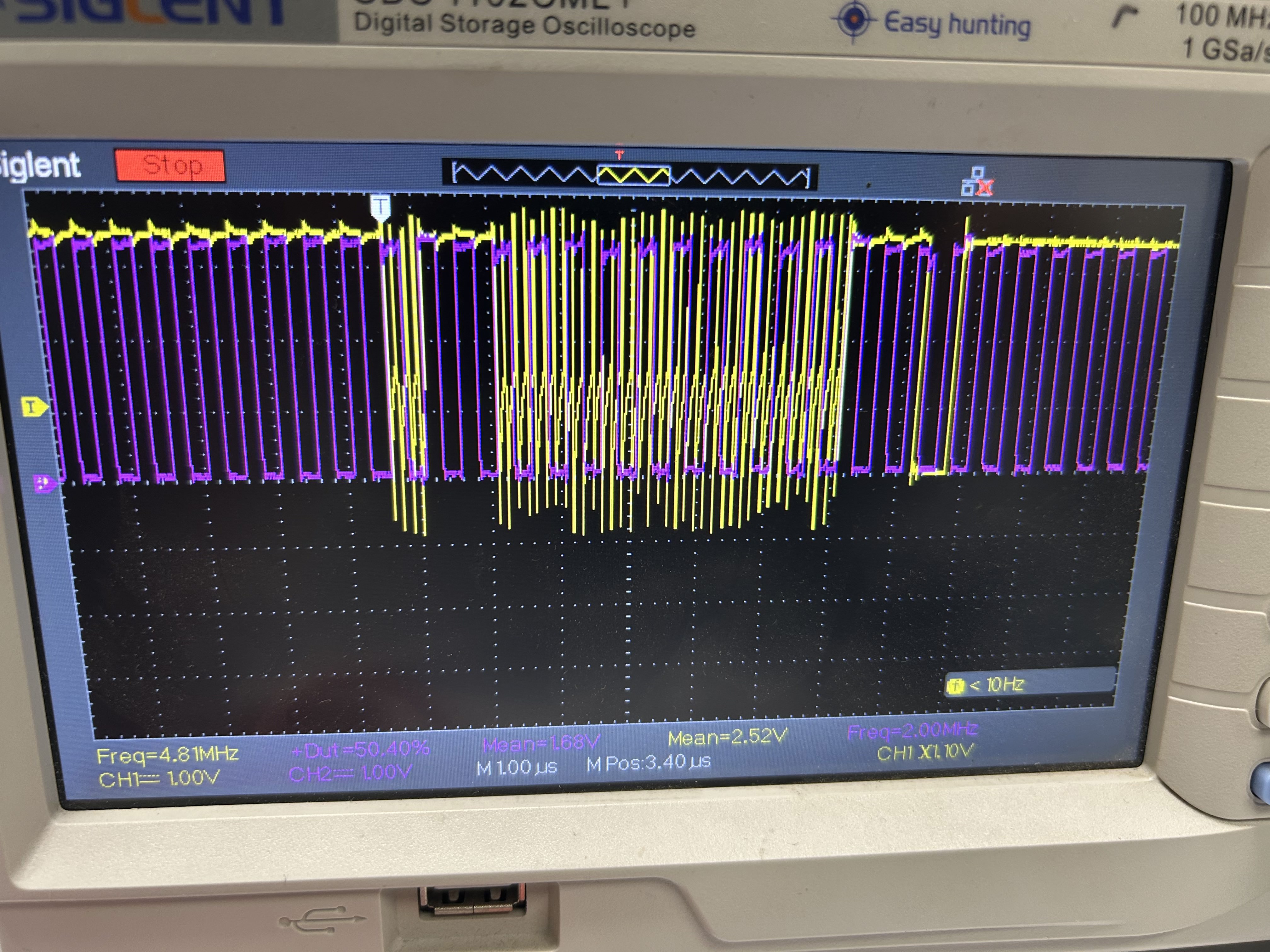
As you suggested, I tried decreasing MDC speed from 1 MHz down to 500KHz down to 250KHz but the behavior was the same. Always those sharp spikes. The MDC clock seems to affect the readings Im getting from the Basic register 1 of the phy, and I think that is because of the issue with the MDIO line since in normal case MDC speed shouldnt affect anything as long as it is under 2.5MHz. Is there some kind of relationship that must me follwed between Core Clock and MDC clock?
I also tried setting up the pull-up feature of PTB4. I tried both pull-up and pull-down but without success. I am curious to know what is the difference between high drive strength, and low drive strength?
Finally Im not sure what you mean by "tuning the MDC frequency" as per my understanding as long as it is under 2.5 MHz it shouldnt matter. Since this line is the only one that is shared between the MAC and the phy for communication I really think theres something up with the electrical behavior of the line when matched with PTB4. Do you have any other ideas of what to test, or any other examples of a similar project done on a S32k148EVB-Q176 that worked?
Thanks for your ongoing support it is very appreciated!
- Mark as New
- Bookmark
- Subscribe
- Mute
- Subscribe to RSS Feed
- Permalink
- Report Inappropriate Content
- Mark as New
- Bookmark
- Subscribe
- Mute
- Subscribe to RSS Feed
- Permalink
- Report Inappropriate Content
It seems I might have been wrong, I just measured the signal on the MDIO line without my PCB plugged in (no phy) meaning that nothing would answer the read request of the MCU and the signal actually looks clean! And it has the same overall form has the bad signal which would mean the phy interaction with the MCU on the MDIO line somehow corrupts the signal of the MCU. See image below
- Mark as New
- Bookmark
- Subscribe
- Mute
- Subscribe to RSS Feed
- Permalink
- Report Inappropriate Content
Ive also measured resistance on the MDIO line between 3.3V and between GND. When I measure only on the phy (not plugged in the nxp board) I get 1.5k ohm to 3.3V and 120k ohm to GND. However if I measure while plugged in the board (not powered) I get 1.5k ohm to 3.3V but 2.9k ohm to GND. I believe the PTB4 might sink it when unpowered but that also means that the MDIO line is fine when not plugged to the board.
- Mark as New
- Bookmark
- Subscribe
- Mute
- Subscribe to RSS Feed
- Permalink
- Report Inappropriate Content
Another thing is in the LAN8720A datasheet, in table 5-12 its written that MDIO signal setup time for data-in in reference to the rising edge of MDC should be at least 10 ns. However, I've measured the signal on the unpowered board with unplugged phy and their seem to be no setup time at all. Is it a parameter I forgot to set? I did set hold time but not setup time. See picture below
- Mark as New
- Bookmark
- Subscribe
- Mute
- Subscribe to RSS Feed
- Permalink
- Report Inappropriate Content
Hello @christopherlajoie ,
Thank you for the detailed follow-up and measurements. Please find answers and suggestions below:
-
The sharp spikes on the MDIO line are indeed unusual. Please try increasing the pull-up resistor to 10 kΩ or higher. A 1.5 kΩ pull-up is not strictly required and may be too aggressive in this case.
-
The S32K148-Q176 board uses TXB0104 bi-directional level shifters between the MCU and the PHY. These can affect signal shape and timing. Please verify their correct operation, as they may be responsible for the ringing or distortion observed on PTB4.
-
Regarding drive strength: setting it to High enables stronger output drivers (more transistors), which improves rise/fall times and increases current capability. This can help with signal integrity, especially on longer traces or capacitive loads. The difference is documented in the S32K1 datasheet.
-
Tuning the MDC frequency means adjusting it to match the electrical characteristics of the MDIO line — including pull-up resistance, trace length, and parasitic capacitance. While MDC can technically run up to 2.5 MHz, lowering it (e.g., to 500 kHz or 250 kHz) can help stabilize marginal signal conditions. However, since you’ve already tried this without improvement, the issue likely lies elsewhere.
-
There is no strict dependency between core clock and MDC clock, other than the fact that MDC is derived from the ENET module clock via the MSCR register. As long as MDC is within spec, the core clock does not directly affect MDIO timing.
Best regards,
Pavel
- Mark as New
- Bookmark
- Subscribe
- Mute
- Subscribe to RSS Feed
- Permalink
- Report Inappropriate Content
Hi Pavel, thanks for this detailed answer. I will try increasing the pull-up resistance to 3.3V line to see if it makes the signal any better.
As for the TXB0104 bi-directional level shifters Im not sure how I can test those, or even where they are found on the board itself. Could you guide me on doing that? Also the board is quite new so I highly doubt it is broken, unless it is defective.
Do you have an input for the setup time question I had? I find it very odd that the MDIO signal doesnt trigger at least 10 ns before the rising edge of MDC as shown in my pictures. Ive set the holdtime parameter to 1 cycle which in my case at 48 MHz equals around 20 ns. It is clearly detailed in the datasheet that setup time must be at least 10 ns. I test for both read and write operation to the phy and neither show a setup time.

Thanks again for your support!
- Mark as New
- Bookmark
- Subscribe
- Mute
- Subscribe to RSS Feed
- Permalink
- Report Inappropriate Content
- Mark as New
- Bookmark
- Subscribe
- Mute
- Subscribe to RSS Feed
- Permalink
- Report Inappropriate Content
Hello @christopherlajoie ,
Thank you for the heads-up regarding your vacation. That gives me sufficient time to prepare a detailed response for you.
Thank you for your update and detailed observations.
Regarding the level shifters for MDIO and MDC signals, please refer to the attached image for the location of U14 (MDIO) and U22 (MDC) on the board (the yellow ones). You can probe their behavior using an oscilloscope to verify signal integrity. I agree that if the board is new, the likelihood of damage is low, unless there is a manufacturing defect.

As for your question about the setup time: on the SMI interface, MDIO is sampled on the next rising edge of MDC. This means that the setup time requirement applies to the data being valid before that edge, not necessarily before the current edge shown in your capture. So the setup time requirement shall be met easily.
To validate the behavior, I ran the lwip_s32k148 example on the S32K148EVB-Q176 board using the following setup:
Software:
- S32 Design Studio v3.5
- SDK: s32sdk_s32k1xx_rtm_401
Hardware:
- TJA1103-SDBR daughter board in rev-RMII mode
- PHY address: 0x02
- No pull-up resistor on MDIO line
I added a PHY driver and defined the PHY entry.

A FreeRTOS task was created to blink an LED and periodically read two PHY registers using PHY_Read(). I kept the MSCR settings at default, resulting in:
- MDC frequency: ~2.39 MHz
- Hold time: 20 ns (MSCR.HOLDTIME = 0x0)
- Hold time: 170 ns (MSCR.HOLDTIME = 0x7 - set by debugger)

I tried resetting the PHY, but it turned out to be unnecessary — so I commented out the related code.
Signals were observed on resistors R46 (MDIO) and R38 (MDC). Below is a waveform capture of a complete Clause 22 read transaction:
- Target PHY: 0x02
- Read register: 0x03
- Data returned by TJA1103: 0xB013 (between cursors)

Please try to capture a full Clause 22 transaction on your oscilloscope for comparison. The waveform should resemble the timing diagram described on Management Data Input/Output - Wikipedia
I'm not able to review your entire code (but thank you for sharing it anyway). However, please note that the first parameter of PHY_Read (as well as other PHY functions) is not the PHY address, but the index of the PHY entry — so it should be 0 or PHY_INSTANCE_0. The PHY address must be set within the PHY entry itself.
Best regards,
Pavel