
- Forums
- Product Forums
- General Purpose MicrocontrollersGeneral Purpose Microcontrollers
- i.MX Forumsi.MX Forums
- QorIQ Processing PlatformsQorIQ Processing Platforms
- Identification and SecurityIdentification and Security
- Power ManagementPower Management
- Wireless ConnectivityWireless Connectivity
- RFID / NFCRFID / NFC
- Advanced AnalogAdvanced Analog
- Neural Processing UnitsNeural Processing Units
- MCX Microcontrollers
- S32G
- S32K
- S32V
- MPC5xxx
- Other NXP Products
- S12 / MagniV Microcontrollers
- Powertrain and Electrification Analog Drivers
- Sensors
- Vybrid Processors
- Digital Signal Controllers
- 8-bit Microcontrollers
- ColdFire/68K Microcontrollers and Processors
- PowerQUICC Processors
- OSBDM and TBDML
- S32M
- S32Z/E
-
- Solution Forums
- Software Forums
- MCUXpresso Software and ToolsMCUXpresso Software and Tools
- CodeWarriorCodeWarrior
- MQX Software SolutionsMQX Software Solutions
- Model-Based Design Toolbox (MBDT)Model-Based Design Toolbox (MBDT)
- FreeMASTER
- eIQ Machine Learning Software
- Embedded Software and Tools Clinic
- S32 SDK
- S32 Design Studio
- GUI Guider
- Zephyr Project
- Voice Technology
- Application Software Packs
- Secure Provisioning SDK (SPSDK)
- Processor Expert Software
- Generative AI & LLMs
-
- Topics
- Mobile Robotics - Drones and RoversMobile Robotics - Drones and Rovers
- NXP Training ContentNXP Training Content
- University ProgramsUniversity Programs
- Rapid IoT
- NXP Designs
- SafeAssure-Community
- OSS Security & Maintenance
- Using Our Community
-
- Cloud Lab Forums
-
- Knowledge Bases
- ARM Microcontrollers
- i.MX Processors
- Identification and Security
- Model-Based Design Toolbox (MBDT)
- QorIQ Processing Platforms
- S32 Automotive Processing Platform
- Wireless Connectivity
- CodeWarrior
- MCUXpresso Suite of Software and Tools
- MQX Software Solutions
- RFID / NFC
- Advanced Analog
- Neural Processing Units
-
- NXP Tech Blogs
- RSS フィードを購読する
- トピックを新着としてマーク
- トピックを既読としてマーク
- このトピックを現在のユーザーにフロートします
- ブックマーク
- 購読
- ミュート
- 印刷用ページ
ADC_DMA
- 新着としてマーク
- ブックマーク
- 購読
- ミュート
- RSS フィードを購読する
- ハイライト
- 印刷
- 不適切なコンテンツを報告
I am using the S32K344 with RTD version 5. I have designed my ADC signal readings to be read in a specific sequence, offset by eMIOS triggers. Currently, I am reading the ADC data using Bctu_Ip_GetFifoData(). The system works as expected, with BCTU_IRQn interrupts for FIFO1 and FIFO2.
Now, I need to switch to DMA, using DMATCD1_IRQn for FIFO1 and DMATCD16_IRQn for FIFO2. The issue I am encountering is that I am unable to read the signals for FIFO2 unless I disable the interrupt for FIFO1, and vice versa. I have attached my project so you can have a closer look at the issue.
- 新着としてマーク
- ブックマーク
- 購読
- ミュート
- RSS フィードを購読する
- ハイライト
- 印刷
- 不適切なコンテンツを報告
Thank you for your interest in our products and for contributing to our community.
Please find attached project.
This example implements two BCTU lists for parallel conversions using ADC0 and ADC1. Each conversion is triggered by a separate PIT channel, and the resulting data is stored in FIFO1 and FIFO2, respectively, as follows:
PIT ch0 -> BCTU List 1 -> FIFO1
ADC0: S10 and VREFL
ADC1: Bandgap and VREFH
PIT ch1 -> BCTU List 2 -> FIFO2
ADC0: VREFH and Bandgap
ADC1: VREFL and S10

Note that ADC channels are used by both ADC instance in both BCTU lists. So S10 with ADC0 is routed to PTD3, meanwhile with ADC1 is routed to on-board potentiometer.
Please use S32DS 3.6, RTD 5.0.0 and S32K3X4EVB-T172.
I hope this information is helpful.
- 新着としてマーク
- ブックマーク
- 購読
- ミュート
- RSS フィードを購読する
- ハイライト
- 印刷
- 不適切なコンテンツを報告
Hi,
Thanks for your response. Based on my previous description, I want to use DMA with a custom design NOT BCTU:
The design I am building is to read ADC data from FIFO1 register using DMA Channel 1 and read ADC data from FIFO2 register using DMA Channel 16, storing both in one software buffer.
- FIFO1 register --> software buffer[21]
- FIFO2 register --> same software buffer, but needs an offset value of the signal number of FIFO1 signals .The Total ADC signals are 21.
Here the main issue:
I have chained Channel 1 and Channel 2, so when Channel 1 completes its major loop, Channel 2 should start transferring the data.
Channel 2 configurations:
- Source: software buffer[21]
- Destination: software buffer[210]
But the system is not working. I have attached my project so you can easily identify the issue. I would appreciate it if you could have a look and find the reason for the issue.
in adddtion to that i aslo have an issue :
Since the destination address [21] for both Channel 1 and Channel 16 is the same, Channel 1 reads 16 signals from FIFO1 and Channel 16 reads 5 signals from FIFO2, totaling 21 signals. How can I offset the destination address for Channel 16 by 16 in the DMA configurations? Currently, I am using a software offset, but I would like to do it in the DMA configurations.

- 新着としてマーク
- ブックマーク
- 購読
- ミュート
- RSS フィードを購読する
- ハイライト
- 印刷
- 不適切なコンテンツを報告
I have not received an answer yet
- 新着としてマーク
- ブックマーク
- 購読
- ミュート
- RSS フィードを購読する
- ハイライト
- 印刷
- 不適切なコンテンツを報告
Hi Ayaz,
seems you had just wrong DMA config, did not enable channel linking and had incorrect Transfer control for DMA channels. See attached modification I did...
Buffers are then filled, not sure if properly as you set system to transfer just raw data

Hope it helps.
BR, Petr
- 新着としてマーク
- ブックマーク
- 購読
- ミュート
- RSS フィードを購読する
- ハイライト
- 印刷
- 不適切なコンテンツを報告
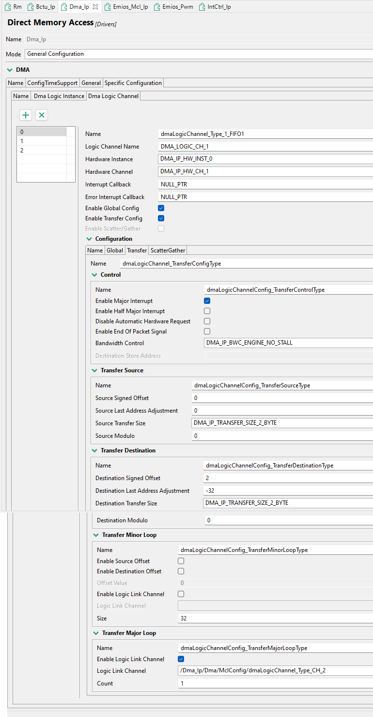
Thanks for your response. It works now.
Now, I have a question regarding the configuration of CH2. The source buffer is an array of 21 signals, but I only want to transfer the first 16 signals into the destination buffer. There will be 10 samples in total, making 160 samples. The destination buffer is of size 160 and uses the unsigned16 data type.
However, in the CH2 configuration, it is possible to transfer 32 bytes at a time, which is my full data per minor loop. So, I have changed my configurations to:
- Source transfer size: 32 bytes
- Destination transfer size: 32 bytes
But it is not working. Do you know the reason? What approach is better? What do you suggest?
New configurations :
the previous approach:


i have attached the project with new configurations
- 新着としてマーク
- ブックマーク
- 購読
- ミュート
- RSS フィードを購読する
- ハイライト
- 印刷
- 不適切なコンテンツを報告
