- Forums
- Product Forums
- General Purpose MicrocontrollersGeneral Purpose Microcontrollers
- i.MX Forumsi.MX Forums
- QorIQ Processing PlatformsQorIQ Processing Platforms
- Identification and SecurityIdentification and Security
- Power ManagementPower Management
- MCX Microcontrollers
- S32G
- S32K
- S32V
- MPC5xxx
- Other NXP Products
- Wireless Connectivity
- S12 / MagniV Microcontrollers
- Powertrain and Electrification Analog Drivers
- Sensors
- Vybrid Processors
- Digital Signal Controllers
- 8-bit Microcontrollers
- ColdFire/68K Microcontrollers and Processors
- PowerQUICC Processors
- OSBDM and TBDML
- S32M
-
- Solution Forums
- Software Forums
- MCUXpresso Software and ToolsMCUXpresso Software and Tools
- CodeWarriorCodeWarrior
- MQX Software SolutionsMQX Software Solutions
- Model-Based Design Toolbox (MBDT)Model-Based Design Toolbox (MBDT)
- FreeMASTER
- eIQ Machine Learning Software
- Embedded Software and Tools Clinic
- S32 SDK
- S32 Design Studio
- GUI Guider
- Zephyr Project
- Voice Technology
- Application Software Packs
- Secure Provisioning SDK (SPSDK)
- Processor Expert Software
- MCUXpresso Training Hub
-
- Topics
- Mobile Robotics - Drones and RoversMobile Robotics - Drones and Rovers
- NXP Training ContentNXP Training Content
- University ProgramsUniversity Programs
- Rapid IoT
- NXP Designs
- SafeAssure-Community
- OSS Security & Maintenance
- Using Our Community
-
- Cloud Lab Forums
-
- Knowledge Bases
- ARM Microcontrollers
- i.MX Processors
- Identification and Security
- Model-Based Design Toolbox (MBDT)
- QorIQ Processing Platforms
- S32 Automotive Processing Platform
- Wireless Connectivity
- CodeWarrior
- MCUXpresso Suite of Software and Tools
- MQX Software Solutions
-
- Home
- :
- 产品论坛
- :
- PowerQUICC处理器
- :
- Re: local memory Map for MPC8358E processor
local memory Map for MPC8358E processor
Please refer to the MPC8360E PowerQUICC II Pro Integrated Communications Processor Family Reference Manual, 4.4.3 System Clock Domains:
"The internal ddr_clk frequency (for DDR) is determined by RCWL[DDRCM]. Note that the lb_clk clock
frequency (for Secondary DDR) is determined by RCWL[LBCM]. See Section 4.3.2.1, “Reset
Configuration Word Low Register (RCWLR).” Note that ddr_clk is not the external memory bus
frequency; ddr_clk passes through the DDR clock divider (÷2) to create the differential DDR memory bus
clock outputs (MCK and MCK). However, the data rate is the same frequency as ddr_clk."
Thank you for replying,
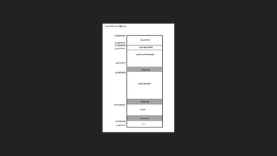
As per MPC8360E PowerQUICC II Pro Integrated Communications Processor Family Reference Manual says, we can put boot flash on All zeros address or 0xFF80_0000 address. can you please elaborate more on this?. so that, my memory mapping is incorrect...
Regards,
Venkat
#RCWLR Value :- 0x02230086
#LBCM-0 LBCM is equal to csb clk (266MHz)
#DDRCM-0 DDRCM is equal to csb clk (266MHz)
#SVCOD-00 system PLL VCO division is 4
#SPMF - 0010 system PLL multiplication factor is 2:1
#COREPLL -0100011 Core freq. 1600MHZ
#CEVCOD -10 QUIIC engine Freq. is 800MHZ
#CEPDF - 0 QUIIC Engine PLL div. factor is 0
#CEPMF- 00110 QUICC engine PLL mortification factor 6
#RCWHR Value :- 0x00600000
#PCIHOST-0 PCI is disable (not using)
#PCIARB-0 PCI arbiter is disable
#PCICKDRV - 0 PCI Buffers are disable
#COEDIS- 0 core can boot without waiting for config. by external master
#BMS- 0 boot memory space is all zeros to 0x007f_ffff
#BOOTSEQ- 00 boot sequencer disabled
#SWEN - 0 Software WDT disable
#ROMLOC- 110 local bus GPCM 16-bit ROM
#SDDRIOE -0 secondary DDR I/O disable
#TLE -0 big-endian mode
#LALE - 0 normal LALE timing
#LDP-0 initial value of SCIRL[LDP_A] is 1 means that LDP0-LDP3 are used for local data parity
Please refer to the MPC8360E PowerQUICC II Pro Integrated Communications Processor Family Reference Manual, 4.4.3 System Clock Domains:
"The internal ddr_clk frequency (for DDR) is determined by RCWL[DDRCM]. Note that the lb_clk clock
frequency (for Secondary DDR) is determined by RCWL[LBCM]. See Section 4.3.2.1, “Reset
Configuration Word Low Register (RCWLR).” Note that ddr_clk is not the external memory bus
frequency; ddr_clk passes through the DDR clock divider (÷2) to create the differential DDR memory bus
clock outputs (MCK and MCK). However, the data rate is the same frequency as ddr_clk."
