- Forums
- Product Forums
- General Purpose MicrocontrollersGeneral Purpose Microcontrollers
- i.MX Forumsi.MX Forums
- QorIQ Processing PlatformsQorIQ Processing Platforms
- Identification and SecurityIdentification and Security
- Power ManagementPower Management
- Wireless ConnectivityWireless Connectivity
- RFID / NFCRFID / NFC
- MCX Microcontrollers
- S32G
- S32K
- S32V
- MPC5xxx
- Other NXP Products
- S12 / MagniV Microcontrollers
- Powertrain and Electrification Analog Drivers
- Sensors
- Vybrid Processors
- Digital Signal Controllers
- 8-bit Microcontrollers
- ColdFire/68K Microcontrollers and Processors
- PowerQUICC Processors
- OSBDM and TBDML
- S32M
-
- Solution Forums
- Software Forums
- MCUXpresso Software and ToolsMCUXpresso Software and Tools
- CodeWarriorCodeWarrior
- MQX Software SolutionsMQX Software Solutions
- Model-Based Design Toolbox (MBDT)Model-Based Design Toolbox (MBDT)
- FreeMASTER
- eIQ Machine Learning Software
- Embedded Software and Tools Clinic
- S32 SDK
- S32 Design Studio
- GUI Guider
- Zephyr Project
- Voice Technology
- Application Software Packs
- Secure Provisioning SDK (SPSDK)
- Processor Expert Software
-
- Topics
- Mobile Robotics - Drones and RoversMobile Robotics - Drones and Rovers
- NXP Training ContentNXP Training Content
- University ProgramsUniversity Programs
- Rapid IoT
- NXP Designs
- SafeAssure-Community
- OSS Security & Maintenance
- Using Our Community
-
- Cloud Lab Forums
-
- Knowledge Bases
- ARM Microcontrollers
- i.MX Processors
- Identification and Security
- Model-Based Design Toolbox (MBDT)
- QorIQ Processing Platforms
- S32 Automotive Processing Platform
- Wireless Connectivity
- CodeWarrior
- MCUXpresso Suite of Software and Tools
- MQX Software Solutions
-
- Home
- :
- QorIQ Processing Platforms
- :
- P-Series
- :
- Re: P2041 Serdes PLL could not work correct
P2041 Serdes PLL could not work correct
- Subscribe to RSS Feed
- Mark Topic as New
- Mark Topic as Read
- Float this Topic for Current User
- Bookmark
- Subscribe
- Mute
- Printer Friendly Page
P2041 Serdes PLL could not work correct
- Mark as New
- Bookmark
- Subscribe
- Mute
- Subscribe to RSS Feed
- Permalink
- Report Inappropriate Content
I use P2041 with LANE H as SGMII and Lane E/F as PCIE-2.
but when cpu bootup,I found SDRDS Register is as Follows:
|---B0RSTCTL = 0x26474507.
|---B1PLLCR0 = 0x0000000c.
|---B1PLLCR1 = 0x08000100.
it means that Serdes is reset failed.
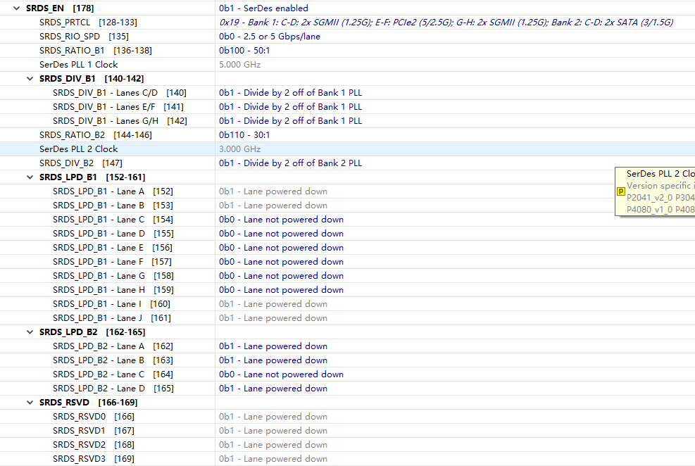
follows is my RCW:
after this,i excute a reset sequence for SRDES,it out put as follows and reset failed at last:
-> serdes_reset
|---B0RSTCTL = 0x26474507.
|---B1PLLCR0 = 0x0000000c.
|---B1PLLCR1 = 0x08000100.
Set SD_RST
|---B0RSTCTL = 0x26474547.
|---B1PLLCR0 = 0x0000000c.
|---B1PLLCR1 = 0x08000100.
SET SDPD and PLLRST
|---B0RSTCTL = 0x26474567.
|---B1PLLCR0 = 0x0000000c.
|---B1PLLCR1 = 0x08000100.
SET RSTREQ
|---B0RSTCTL = 0x06474562.
|---B1PLLCR0 = 0x0000000c.
|---B1PLLCR1 = 0x08000100.
Clear SD_RST SDPD and PLLRST
|---B0RSTCTL = 0x06474504.
|---B1PLLCR0 = 0x0000000c.
|---B1PLLCR1 = 0x08000100.
value = 27 = 0x1b
-> serdes_dump
|---B0RSTCTL = 0x26474507.
|---B1PLLCR0 = 0x0000000c.
|---B1PLLCR1 = 0x08000100.
value = 27 = 0x1b
- Mark as New
- Bookmark
- Subscribe
- Mute
- Subscribe to RSS Feed
- Permalink
- Report Inappropriate Content
会不会是焊接问题导致的?
- Mark as New
- Bookmark
- Subscribe
- Mute
- Subscribe to RSS Feed
- Permalink
- Report Inappropriate Content
Please provide:
1) U-Boot log as text attachment
2) SerDes reference clocks frequencies
- Mark as New
- Bookmark
- Subscribe
- Mute
- Subscribe to RSS Feed
- Permalink
- Report Inappropriate Content
hi,ufedor!
My operation system is vxWorks,no u-boot.
Serder reference clocks is 100M.
thanks...
- Mark as New
- Bookmark
- Subscribe
- Mute
- Subscribe to RSS Feed
- Permalink
- Report Inappropriate Content
> Serder reference clocks is 100M.
Both reference clocks or one?
If one - which exactly SD_REF_CLK1 or SD_REF_CLK2?
Please provide RCW in either form:
- text file of the RCW dump
- binary image
- Mark as New
- Bookmark
- Subscribe
- Mute
- Subscribe to RSS Feed
- Permalink
- Report Inappropriate Content
Yes,both SD_REF_CLK is 100M。
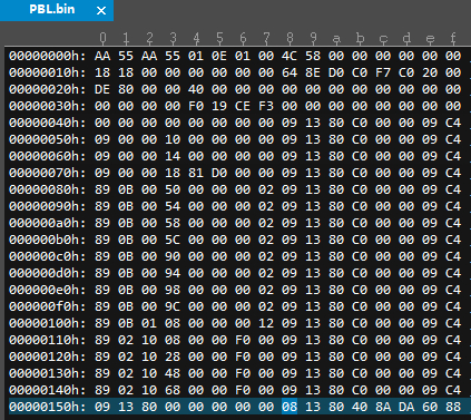
RCW is as follows:
- Mark as New
- Bookmark
- Subscribe
- Mute
- Subscribe to RSS Feed
- Permalink
- Report Inappropriate Content
Excuse me, by it was written "text file".
This means - not picture.
- Mark as New
- Bookmark
- Subscribe
- Mute
- Subscribe to RSS Feed
- Permalink
- Report Inappropriate Content
sorry! by the way, system do not have sd_ref_clk_2.
0xf8000000: aa 55 aa 55 01 0e 01 00 4c 58 00 00 00 00 00 00
0xf8000010: 18 18 00 00 00 00 00 00 64 8e d0 c0 f7 c0 20 00
0xf8000020: de 80 00 00 40 00 00 00 00 00 00 00 00 00 00 00
0xf8000030: 00 00 00 00 f0 19 ce f3 00 00 00 00 00 00 00 00
0xf8000040: 00 00 00 00 00 00 00 00 09 13 80 c0 00 00 09 c4
0xf8000050: 09 00 00 10 00 00 00 00 09 13 80 c0 00 00 09 c4
0xf8000060: 09 00 00 14 00 00 00 00 09 13 80 c0 00 00 09 c4
0xf8000070: 09 00 00 18 81 d0 00 00 09 13 80 c0 00 00 09 c4
0xf8000080: 89 0b 00 50 00 00 00 02 09 13 80 c0 00 00 09 c4
0xf8000090: 89 0b 00 54 00 00 00 02 09 13 80 c0 00 00 09 c4
0xf80000a0: 89 0b 00 58 00 00 00 02 09 13 80 c0 00 00 09 c4
0xf80000b0: 89 0b 00 5c 00 00 00 02 09 13 80 c0 00 00 09 c4
0xf80000c0: 89 0b 00 90 00 00 00 02 09 13 80 c0 00 00 09 c4
0xf80000d0: 89 0b 00 94 00 00 00 02 09 13 80 c0 00 00 09 c4
0xf80000e0: 89 0b 00 98 00 00 00 02 09 13 80 c0 00 00 09 c4
0xf80000f0: 89 0b 00 9c 00 00 00 02 09 13 80 c0 00 00 09 c4
0xf8000100: 89 0b 01 08 00 00 00 12 09 13 80 c0 00 00 09 c4
0xf8000110: 89 02 10 08 00 00 f0 00 09 13 80 c0 00 00 09 c4
0xf8000120: 89 02 10 28 00 00 f0 00 09 13 80 c0 00 00 09 c4
0xf8000130: 89 02 10 48 00 00 f0 00 09 13 80 c0 00 00 09 c4
0xf8000140: 89 02 10 68 00 00 f0 00 09 13 80 c0 00 00 09 c4
0xf8000150: 09 13 80 00 00 00 00 00 08 13 80 40 8a da 60 88
- Mark as New
- Bookmark
- Subscribe
- Mute
- Subscribe to RSS Feed
- Permalink
- Report Inappropriate Content
> by the way, system do not have sd_ref_clk_2.
In this case SRDS_LPD_B2 - Lane C has to be powered down.
- Mark as New
- Bookmark
- Subscribe
- Mute
- Subscribe to RSS Feed
- Permalink
- Report Inappropriate Content
thanks for your answer.
I set the lane C to power down.but it's still not work.new RCW is as follows:
0xf8000000: aa 55 aa 55 01 0e 01 00 4c 58 00 00 00 00 00 00
0xf8000010: 18 18 00 00 00 00 00 00 64 8e d0 c0 ff c0 20 00
0xf8000020: de 80 00 00 40 00 00 00 00 00 00 00 00 00 00 00
0xf8000030: 00 00 00 00 f0 19 ce f3 00 00 00 00 00 00 00 00
0xf8000040: 00 00 00 00 00 00 00 00 09 13 80 c0 00 00 09 c4
0xf8000050: 09 00 00 10 00 00 00 00 09 13 80 c0 00 00 09 c4
0xf8000060: 09 00 00 14 00 00 00 00 09 13 80 c0 00 00 09 c4
0xf8000070: 09 00 00 18 81 d0 00 00 09 13 80 c0 00 00 09 c4
0xf8000080: 89 0b 00 50 00 00 00 02 09 13 80 c0 00 00 09 c4
0xf8000090: 89 0b 00 54 00 00 00 02 09 13 80 c0 00 00 09 c4
0xf80000a0: 89 0b 00 58 00 00 00 02 09 13 80 c0 00 00 09 c4
0xf80000b0: 89 0b 00 5c 00 00 00 02 09 13 80 c0 00 00 09 c4
0xf80000c0: 89 0b 00 90 00 00 00 02 09 13 80 c0 00 00 09 c4
0xf80000d0: 89 0b 00 94 00 00 00 02 09 13 80 c0 00 00 09 c4
0xf80000e0: 89 0b 00 98 00 00 00 02 09 13 80 c0 00 00 09 c4
0xf80000f0: 89 0b 00 9c 00 00 00 02 09 13 80 c0 00 00 09 c4
0xf8000100: 89 0b 01 08 00 00 00 12 09 13 80 c0 00 00 09 c4
0xf8000110: 89 02 10 08 00 00 f0 00 09 13 80 c0 00 00 09 c4
0xf8000120: 89 02 10 28 00 00 f0 00 09 13 80 c0 00 00 09 c4
0xf8000130: 89 02 10 48 00 00 f0 00 09 13 80 c0 00 00 09 c4
0xf8000140: 89 02 10 68 00 00 f0 00 09 13 80 c0 00 00 09 c4
0xf8000150: 09 13 80 00 00 00 00 00 08 13 80 40 89 e0 dd 1f
the serder pll reset output message as follows:
-> serdes_reset
|---B0RSTCTL = 0x26474507.
|---B1PLLCR0 = 0x0000000c.
|---B1PLLCR1 = 0x08000100.
Set SD_RST
|---B0RSTCTL = 0x26474547.
|---B1PLLCR0 = 0x0000000c.
|---B1PLLCR1 = 0x08000100.
SET SDPD and PLLRST
|---B0RSTCTL = 0x264745e7.
|---B1PLLCR0 = 0x0000000c.
|---B1PLLCR1 = 0x08000100.
SET RSTREQ
|---B0RSTCTL = 0x064745e1.
|---B1PLLCR0 = 0x0000000c.
|---B1PLLCR1 = 0x08000100.
|---B0RSTCTL = 0x064745e4.
|---B1PLLCR0 = 0x0000000c.
|---B1PLLCR1 = 0x08000100.
|---B0RSTCTL = 0x064745e4.
|---B1PLLCR0 = 0x0000000c.
|---B1PLLCR1 = 0x08000100.
|---B0RSTCTL = 0x064745e4.
|---B1PLLCR0 = 0x0000000c.
|---B1PLLCR1 = 0x08000100.
|---B0RSTCTL = 0x264745e7.
|---B1PLLCR0 = 0x0000000c.
|---B1PLLCR1 = 0x08000100.
|---B0RSTCTL = 0x264745e7.
|---B1PLLCR0 = 0x0000000c.
|---B1PLLCR1 = 0x08000100.
|---B0RSTCTL = 0x264745e7.
|---B1PLLCR0 = 0x0000000c.
|---B1PLLCR1 = 0x08000100.
|---B0RSTCTL = 0x264745e7.
|---B1PLLCR0 = 0x0000000c.
|---B1PLLCR1 = 0x08000100.
|---B0RSTCTL = 0x264745e7.
|---B1PLLCR0 = 0x0000000c.
|---B1PLLCR1 = 0x08000100.
|---B0RSTCTL = 0x264745e7.
|---B1PLLCR0 = 0x0000000c.
|---B1PLLCR1 = 0x08000100.
Clear SD_RST SDPD and PLLRST
|---B0RSTCTL = 0x26474507.
|---B1PLLCR0 = 0x0000000c.
|---B1PLLCR1 = 0x08000100.
LAST Status.
|---B0RSTCTL = 0x26474507.
|---B1PLLCR0 = 0x0000000c.
|---B1PLLCR1 = 0x08000100.
- Mark as New
- Bookmark
- Subscribe
- Mute
- Subscribe to RSS Feed
- Permalink
- Report Inappropriate Content
> the serder pll reset output message as follows:
What are the following lines?
Have you programmed the RCW into a Flash?
- Mark as New
- Bookmark
- Subscribe
- Mute
- Subscribe to RSS Feed
- Permalink
- Report Inappropriate Content
thanks for all your reply,do you have some document to explain how configure SerDer and Debug it.
- Mark as New
- Bookmark
- Subscribe
- Mute
- Subscribe to RSS Feed
- Permalink
- Report Inappropriate Content
SerDes parameters have to be configured in accordance with the QorIQ P2040 Reference Manual descriptions:
Table 3-13. SerDes Lane Multiplexing/Configuration
Table 4-14. Valid SerDes RCW Encodings and Reference Clocks
There are no additional documents concerning SerDes debugging.
Usually RCW is programmed into the boot Flash and tested by powering-on the board.
No additional debug or software control is needed because SerDes is configured by internal microcode using RCW data during POR sequence.
- Mark as New
- Bookmark
- Subscribe
- Mute
- Subscribe to RSS Feed
- Permalink
- Report Inappropriate Content
Table 3-13. SerDes Lane Multiplexing/Configuration : I select 0x19 for use SGMII 4 for dtsec and PCIE2.
Table 4-14. Valid SerDes RCW Encodings and Reference Clocks: Ratio set 50:1 and set DIV to /2.
did some error in my RCW.
why SerDes PLL always could not lock?
thanks!
- Mark as New
- Bookmark
- Subscribe
- Mute
- Subscribe to RSS Feed
- Permalink
- Report Inappropriate Content
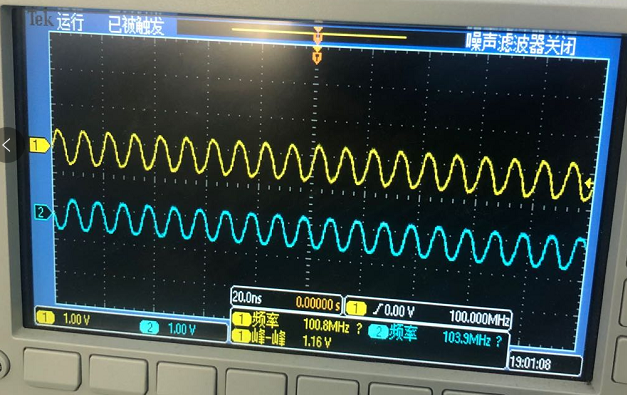
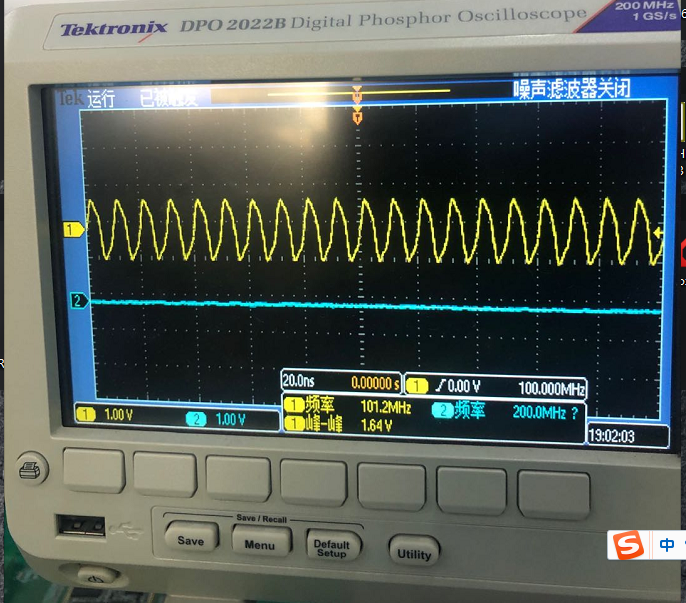
Use a digital scope and provide traces of the SD_REF_CLK1 at the processor's pins.
- Mark as New
- Bookmark
- Subscribe
- Mute
- Subscribe to RSS Feed
- Permalink
- Report Inappropriate Content
PIC1:REF_CLK_P and REF_CLK_N On each channel
PIC2: REF_CLK_P On oscilloprobe's GND and REF_CLK_N on oscilloprobe's signal pin
- Mark as New
- Bookmark
- Subscribe
- Mute
- Subscribe to RSS Feed
- Permalink
- Report Inappropriate Content
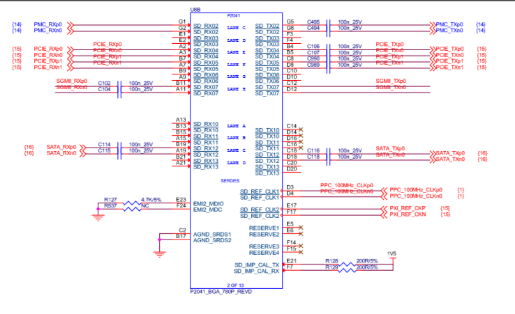
Please provide complete processor connection schematics as PDF.
- Mark as New
- Bookmark
- Subscribe
- Mute
- Subscribe to RSS Feed
- Permalink
- Report Inappropriate Content
Sorry I can not provide whole schematics as PDF,follwos is main schematics about clock src and signals to CPU:
- Mark as New
- Bookmark
- Subscribe
- Mute
- Subscribe to RSS Feed
- Permalink
- Report Inappropriate Content
ufedor Could you give me some advise?thanks...
- Mark as New
- Bookmark
- Subscribe
- Mute
- Subscribe to RSS Feed
- Permalink
- Report Inappropriate Content
I've already sent you response from the corresponding Technical Case.
I'm waiting for the complete processor connection schematics.
- Mark as New
- Bookmark
- Subscribe
- Mute
- Subscribe to RSS Feed
- Permalink
- Report Inappropriate Content
How can I send you the schematics?
